Hi Dave,
In other words, it is more like star-on-star grounding in a tree-like structure. I always try to be aware of where the currents are flowing and what paths they are taking, especially where the bad currents may be high, as in the output stage. I am a big believer in multiple layers of R-C decoupling as the rails progress back toward the VAS and input stages.
Cheers,
Bob
I agree and these are all good points.
I like to use star grounding in the part of the amp that have "clean" currents like in the frontend, "VAS" and driverstage running in class A.
Where you have "dirty" currents I like to use a ground plane.
Stein
Last edited:
Hello Bob
First of all let me congratulate you on your work and Book that I keep as a reference.
I just finished building the RCP130 GAIA DIFPAIRVAS power amp that is based on the design Figure 9.15 page 209 of the second edition of your Book.
My implementation uses much higher LTP tail current and lower source degeneration.
Would you care to explain why you chose only 2mA and 470ohm in those places ?
My work is explained here: https://www.diyaudio.com/forums/sol...ral-mosfet-power-amplifier-3.html#post6763678
It would be an honour to have your comments there also.
Attachments
Hi Ricardo,
Using 2 mA was a fairly arbitrary choice, and the size of the degeneration resistors follows my usual rule of thumb to have 10:1 degeneration in the input pair (in this case Rs ~ 9X 1/gm of the LSK389 JFET operating at 1 mA each).
That having been said, I probably indeed left some SNR on the table, and if I had it to do over again I would increase the current as well, especially given the use of the LSK389 whose noise will be lower at 2X or 4X the current, but I would still adjust the the source resistors to keep 10:1 degeneration. Those changes would indeed reduce the noise somewhat, assuming that the input pair and its degeneration resistors is the main source of noise. So I agree with you on increasing the current. Running the LSK389s in this arrangement at more than 4 mA each begins to approach the point of diminishing returns.
Importantly, increasing the current in the manner described above increases the transconductance of the IPS, so the Miller compensation capacitor needs to be increased to keep the gain crossover frequency the same. These actions alone may not end up increasing the slew rate much at the end of the day, since you have increased the IPS transconductance and as a result need to increase the Miller capacitance. However, some advantage is achieved because increasing the current in the JFET only increases the gm by the square root (unlike a BJT). If you quadruple the bias current, in theory the gm will only double and the Miller capacitance will only double, and yet in principle you will have 4X the current to charge and discharge the Miller capacitor if that is the dominant limitation on achievable slew rate.
I also notice that you made some changes in the compensation which can allow stability with a higher gain crossover frequency if done carefully. Some times these useful tricks can introduce some real-world stability risk, especially in regard to gain margin. Err on the conservative side, here. Simulations can sometimes be overly optimistic in the results they give on gain and phase margin. Also, be especially aware of the effect that the gate stopper resistors for the MOSFETs have on phase lag, and this is often not modeled that well. Also be aware that the MOSFET capacitances can change with the operating point. Watch carefully for parasitic oscillation bursts on the back porch of a high-amplitude sine wave, including with different load resistances.
It does look like you have put a lot of good thought into this design.
Cheers,
Bob
Thank you for your insight Bob.
In fact I increased the current to lower noise principally but also because I know this IPS that I use in other builds and the values chosen have been proven in the past.
Decreasing source degen below 100ohm makes bass become snappy but highs become too sharp. Increasing degen to 120 softens the sound too much.... 100 is my best choice.
I will test for your rule of thumb to have 10:1 degeneration in the input pair and see how far off I am now.
As for compensation, I followed my previous experiences and indeed it works very well.
This design is a step forward when compared to the LIN topology.... I wonder how should sound your design of page210.....
As you know I built a modular power amp where I can easily swap the input stages so I will have a go at that design also.
Just to finish I have a special question:
In my designs I use led referenced CCS and I always tend to use large capacitors to filter the leds..... It would be easier (less parts and less cap signature) if I could use the leds without local filtering.... Do you believe this is feasible ?
Just to finish I have a special question:
In my designs I use led referenced CCS and I always tend to use large capacitors to filter the leds..... It would be easier (less parts and less cap signature) if I could use the leds without local filtering.... Do you believe this is feasible ?
I haven't had a problem with noise in LED-referenced current sources. In an LTP, the CCS noise is common-mode and will be attenuated by the mirror or, if you use a differential VAS, by the second stage CMRR. Trying to filter an LED directly seems pointless because the dynamic impedance of the LED is much lower than that of the capacitor, especially at low frequencies where the noise is greatest. You can isolate the LED with an RC low-pass filter, but then you are losing the low impedance advantage.
Edit: I notice you ditched the input stage common-mode control loop in favor of a buffered current mirror. Perfectly legit choice, but I think Bob's common-mode circuit is extremely clever and elegant and solves the problem of defining where the diff amp collectors sit. I don't have the book, but I have read the paper on Bob's site. You've added cascodes to the input pair. Bob's circuit seems to have an advantage in controlling the operating points of both the cascodes and the tong-tail pair.
Last edited:
A related question, and perhaps someone will respond. I've been adapting the error-correcting front end to a headphone amplifier circuit. I recently finished a headphone amplifier based on the Blameless topology and had trouble with how it clips. I posted about it here: New Headphone Amplifier Design
Playing around with SPICE yesterday, I came up with the attached circuit. This is just a starting point, please be gentle.
I found that adding the driven cascode greatly reduces distortion, but the simulated loop gain becomes impossibly high, around 140 dB. I knocked this down by degenerating the sources with 1K resistors. I also switched to global three-pole compensation and the Bode plots seem promising.
1K is roughly in the range of ten times 1/gm, but is on the high side by convention. Notwithstanding the noise contribution, I'm wondering if there's any other serious problems with running such large source resistors.
Attachments
Playing around with SPICE yesterday, I came up with the attached circuit. This is just a starting point, please be gentle.
😉
Maybe it's time to try inverting config with something an order of 2k input impedance?
😉
Maybe it's time to try inverting config with something an order of 2k input impedance?
LOL, anything is possible at this point. I'm just exploring.
I had never tried TPC before. The Blameless headphone amp has very high OLG as well and I was seriously expecting to build a power oscillator. To my amazement, it's very stable and required no compensation tuning from the first iteration. I don't have the equipment to measure gain/phase so I have to trust SPICE and then it either oscillates when I build it or it doesn't.
I found a compensation formula that's stable in simulation with 100 Ohm source resistors. But 140 dB of loop gain freaks me out, and the phase margin is only six or seven degrees at midband. I know phase is allowed to go negative in conditionally stable amplifiers, but I don't like the smell of it.
I need to do some noise analysis and see whether or not this is a problem. This isn't a microphone amplifier, after all.
Edit: I may have missed part of the joke. I guess the point is why worry about a 1K resistor when the signal source impedance is more than double that? I'm a little slow on the uptake, but I have this notion that current noise is lower in JFETs than in BJTs, so the noise contribution of the JFET stage will be less dependent on source lead resistance. But I haven't studied it enough yet to know if that intuition is correct.
Last edited:
At super high gains there is scope for unintended (positive) feedback paths through supply rails and poor decoupling or layout mistakes, which can be invisible to standard stability analysis of just the conventional signal path.But 140 dB of loop gain freaks me out
Its possible to simulate closer to this level of detail by including the wiring as resistors of a few milliohms, and representing the source impedance of the actual supply realistically.
At super high gains there is scope for unintended (positive) feedback paths through supply rails and poor decoupling or layout mistakes, which can be invisible to standard stability analysis of just the conventional signal path.
Makes sense, thanks.
I don't have the equipment to measure gain/phase so I have to trust SPICE and then it either oscillates when I build it or it doesn't.
I generally trust impulse or square wave response in the built amplifier. General stability is determined by damping, as seen is settling time, overshoot (if any), and ringing (if any) If you see no overshoot or ringing, linear system theory says you have 60 deg or better phase margin.
The rub here is that the theory is for two pole systems, and our amplifiers have lots more poles than that, and the poles move the large signal voltage and current in the amplifier at any given point. Try to exercise things so that transistors approach saturation. Secondary, tertiary, and higher order poles will shift down by an order of magnitude or more as the transistor associated with that pole nears saturation.
Look for fuzz at the tops and bottoms of sine waves. If you could superimpose a small square wave onto a low frequency large sine wave, that would be really useful for observing the large signal stability of an amp.
These are all very good points. The SPICE models often don't do a good job of modeling ft droop at high current and/or low Vce.
Cheers,
Bob
Cheers,
Bob
I ended up building the amplifier and got it running about six weeks ago. It handles square waves and clipping and overdrive without any tendency at all to misbehave. Overall, it's a different design from the one in Mr. Cordell's paper, but the basic architecture of the front end is identical. I'm sure that's why it works so well. I'm also very happy with how it plays music.
Oh, yes, I forgot: I ended up going with 470 Ohm source resistors in the input stage and there are no issues with noise or otherwise.
I generally trust impulse or square wave response in the built amplifier.
For me square wave response provides more useful information than measuring THD figures.
For me square wave response provides more useful information than measuring THD figures.
They are both important, and often are orthogonal. A solid state amplifier with a beautiful square wave response and 1% THD due to crossover distortion is a piece of crap.
Cheers,
Bob
I ended up building the amplifier and got it running about six weeks ago. It handles square waves and clipping and overdrive without any tendency at all to misbehave. Overall, it's a different design from the one in Mr. Cordell's paper, but the basic architecture of the front end is identical. I'm sure that's why it works so well. I'm also very happy with how it plays music.
Oh, yes, I forgot: I ended up going with 470 Ohm source resistors in the input stage and there are no issues with noise or otherwise.
Nice! Can we see a schematic?
Cheers,
Bob
very nice
That's really nice looking, a clean, tidy (happy) chassis,
is a good sounding and testing chassis.
Few surprises there.
I love the symmetry and layout... KUDOS!
I ended up building the amplifier and got it running about six weeks ago.
I'm also very happy with how it plays music.
That's really nice looking, a clean, tidy (happy) chassis,
is a good sounding and testing chassis.
Few surprises there.
I love the symmetry and layout... KUDOS!
Any testing with a reactive load?
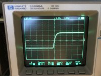
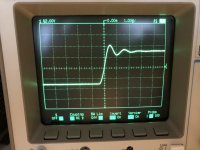
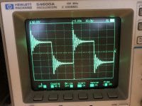
20kHz square wave, 50 Ohm load, 3V peak. No parallel cap, 0.01uF, and 0.1uF, respectively.
In a separate test, I measured the slew rate at 50V/uS. I forget the bandwidth. It has an ultrasonic filter, is -3dB at several hundred kilohertz with the volume control full open.
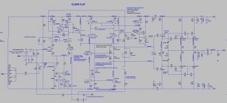
Bob, I will post details of the circuit later this afternoon.
Attachments
Last edited:
- Home
- Amplifiers
- Solid State
- Bob Cordell's Power amplifier book