Notwithstanding its popularity, the double emitter-follower output stage is significantly inferior to the Locanthi-type triple emitter-follower output stage in virtually all respects.
Hi Worldie,
In some cases, a diamond buffer in front of the output transistors is even better. See for example fig. 17.
Cheers, E.
Hi Edmond,
Why do you need triple with mosfet OPS or EC to get very low THD?😉
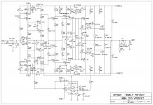
My CFA with IRFP240/9240 has less then 3ppm at 20kHz and full output power with simple OPS and two pole compensation, OITPC.
By the way, I changed output mosfet protection that one was not good enough, moved zeners after mosfets gate resistors.
Why do you need triple with mosfet OPS or EC to get very low THD?😉
My CFA with IRFP240/9240 has less then 3ppm at 20kHz and full output power with simple OPS and two pole compensation, OITPC.
By the way, I changed output mosfet protection that one was not good enough, moved zeners after mosfets gate resistors.
Attachments
Last edited:
Hi Worldie,
In some cases, a diamond buffer in front of the output transistors is even better.
I confess I have never examined the "diamond buffer".
Hi Edmond,
Why do you need triple with MOSFET OPS or EC to get very low THD?
There may be no need to have a double-emitter follower preceding a complementary MOSFET output stage -- a single complementary emitter follower may suffice, as you have indicated; however, with BJT output transistors, a double-emitter follower arrangement is sub-optimal, especially if the amplifier is expected to drive adverse loads (<4Ohms).
Why triple?
Why a triple (or a diamond triple)? Because the gain of the Super TIS heavily relies on the output impedance of this TIS, paralleled by the input impedance of the next (i.e. output) stage. Remember, the current gain of this TIS itself is just 1x. So sufficient loop gain has to be created by other means (i.e. high impedance).
Cheers, E.
Hi Damir,Hi Edmond,
Why do you need triple with mosfet OPS or EC to get very low THD?😉
My CFA with IRFP240/9240 has less then 3ppm at 20kHz and full output power with simple OPS and two pole compensation, OITPC.
By the way, I changed output mosfet protection that one was not good enough, moved zeners after mosfets gate resistors.
Why a triple (or a diamond triple)? Because the gain of the Super TIS heavily relies on the output impedance of this TIS, paralleled by the input impedance of the next (i.e. output) stage. Remember, the current gain of this TIS itself is just 1x. So sufficient loop gain has to be created by other means (i.e. high impedance).
Cheers, E.
How so? By demonstrating that some of the truths expounded here about the interplay of VAS parameters to amplifier distortion aren't, as a matter of fact, universally true?
Like it or not, in the world of discrete audio power amplifiers the double EF, despite its limitations, is probably the most ubiquitous bipolar power output stage out there.
The preponderance of the double EF output stage doesn't mean it is better or the best - it just means it is cheaper.
Cheers,
Bob
Whether degeneration vas is worth or not, should be very easy to verify. Just put a bypass cap across the degeneration resistor and run simulation. It may defer amp by amp, and get deferent conclusions.
PS: do not try this outside simulation. You will disable current protection by doing this.
PS: do not try this outside simulation. You will disable current protection by doing this.
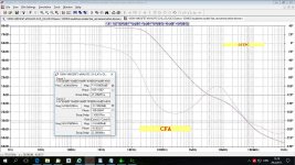
Just for the sake of it, attached is a quick sim of a typical 100W / 4 ohm "Blameless" amplifier with a global ULGF of ~830 kHz. The VAS emitter degeneration was stepped from 0 to 200 R in 50 R increments. For each value of degeneration the THD was taken at 1/2/5 frequency intervals from 20Hz to 20kHz.
The ratio of highest to lowest distortion (over the range of degeneration) is greatest at the lowest audio octaves, which is exactly as one should expect. This is because the most important parameter of the VAS, as far as its ability to drive the non-linear load of the power output stage is concerned, is its ability to keep its output impedance low. At low frequencies feedback via the Miller-feedback compensation capacitor is minimal and you're now relying on on the VAS transconductance being as high as it can be to keep the Miller-feedback loop gain up.
Howdy mate
How is life down under?
I hope that when you stepped R19 you made sure that the standing current in the VAS was constant, by stepping at least R20.
Did you also run an open loop AC simulation when you stepped the VAS emitter degen R to look at the stability?
Stein
Hi Worldie,
In some cases, a diamond buffer in front of the output transistors is even better. See for example fig. 17.
Cheers, E.
Yes I agree.
I have used Diamond triple OPS for many years.
Stein
There was talk of making the BC-1 available as a PCB set or maybe as Gerbers.
Did anything come of this?
Did anything come of this?
Hi Dave,
I have been working with Bob to get a BC-1 pcb set put together. We have the first rev of pcbs running and integrated into a modushop 3Ux300mm dissipante chassis. Basically working on finalizing the design details. So far we have 4 pcbs done for testing, afe, ops, protection, and a power supply. Bob has tested afe and ops. I have tested the power supply, we have to test the protection ckt still. Pcbs will probably be released as a set to purchase similar to what we did for DH-220c. Working on a release for later in the year since it being summer now for me, I am busy doing construction and other outdoors activities while the weather is nice and warm. Sorry it is taking so long but it is nearing completion.
A few chassis details need to be sorted out like chassis/signal grounding , Ac supply, power switch location, do we need a soft-start ckt? My idea is to present a finished reference design that makes sourcing components and assembly as easy as possible with links to Mouser shopping carts and documents, pics of assembly on a cloud link, same as DH-220c,500c designs.
Rick
Last edited:
There's free Gerbers here on diyAudio, for a soft start PCB with bypass. The board also lets you use a low voltage + low current on/off switch on the front panel (5VDC @ 5mA). It supports both "toggle" switches, and "momentary" switches (push-on, push-off) on the front panel. Board name is H9KPXG.
Hi Mark,
Yes I am aware of them but it is good to make everyone else aware. My issue would be how to fit them into the chassis as room is getting sparce. It’s the mechanical bits that are the challenges in getting it all done.
Yes I am aware of them but it is good to make everyone else aware. My issue would be how to fit them into the chassis as room is getting sparce. It’s the mechanical bits that are the challenges in getting it all done.
Thanks Rick. That looks very comprehensive!
I was thinking of starting my own layout if there was not already one, but happy to wait a while. Especially for an approved layout.
I am interested in this because I have built a lot of amps and my favourite is still the Leach lowTIM. I have a feeling that the triple o/p stage is one of the reasons. The BC-1 looks like a modern version.
May I ask if you will separately route the decoupling returns, like the Leach 4.5 layout?
(I like the look of Bob's decoupling hierachy!).
Best regards,
Dave
Hi Dave,
I'm not familiar with the Leach layout, but the BC-1 does follow the decoupling approach I describe in my book. In other words, it is more like star-on-star grounding in a tree-like structure. I always try to be aware of where the currents are flowing and what paths they are taking, especially where the bad currents may be high, as in the output stage. I am a big believer in multiple layers of R-C decoupling as the rails progress back toward the VAS and input stages.
The BC-1 is coming along very well. As Rick says, the mechanical/physical design can eat up a lot of time, especially when you seek to make it something that others can build and with a nice enclosure.
Cheers,
Bob
Hi Bob,
The (single layer) layout can be found here:
http://leachlegacy.ece.gatech.edu/lowtim/cmpt1.html
I had to print this off and highlight the 0V tracks to work out what he had done, however don't spend time on it because it sounds like you have moved to the next level.
If it helps a quick perusal: The left hand side "Central Ground is for the decoupling caps and the RHS "signal/central ground" is for the circuit 0Vs. They are commoned at the power star.
Cheers,
Dave
PS, I agree it's a LOT of work!
Thanks, Dave.
One thing that I often do for bypass capacitor pairs that go to the 2 rails and ground is to connect them together first, then run a shot trace to the ground spine. The idea is that rail-rail noise currents through the caps gets resolved before entering the ground bus. This is especially important for the two caps that are on the board right at the rails where the power transistors connect to the rails. In cases where a ground plane or large power island is used, I also tend to do this to keep the nasty currents from circulating in the ground plane or island.
Speaking of the work Rick and I are doing on the BC-1, our joint construction article on the DH-220C was just published in the July and August issues of audioXpress.
Cheers,
Bob
Hi Edmond,
Why do you need triple with MOSFET OPS or EC to get very low THD?
With error feedback correction, you will, in fact, need a quadruple output stage for optimal performance, irrespective of the output devices used -- MOSFETs or BJTs.
- Home
- Amplifiers
- Solid State
- Bob Cordell's Power amplifier book