Yes, BJT's can be used for the cascode. However, it is true that there is a rather slight noise advantage with JFETs in the cascode because there is no base current to contribute to the noise. With a JFET cascode virtually ALL of the signal current from below into the source ends up at the drain.
Incidentally, BJTs usually are available with significantly higher voltage ratings than JFETs, the latter often available with only a 40-V or so rating. If you use JFETs in the input stage of a conventional Thompson power amplifier that has high rail voltages of, say 65 V, you will likely need BJT cascodes to cope with the higher rail voltage. As an example, it is common to bias the BJT cascode bases at +15 V, in which case the BJT cascodes would have on the order of 48-50 V across them with a 65 V rail.
Cheers,
Bob
I have been using depletion mode Mosfets for the cascode biased from the source of the Jfets for some time. Works well and you can get 350V parts DN2535 - Depletion Mode MOSFETs. Unfortunately no P channel depletion mode devices that I know of.
Neat idea. What is their Vgs at 2 mA?
Do you try to match them? Vgs can be all over the place for MOSFETs, and if their Vgs is too far apart, the input JFETs will see different drain voltages.
Cheers,
Bob
Do you try to match them? Vgs can be all over the place for MOSFETs, and if their Vgs is too far apart, the input JFETs will see different drain voltages.
Cheers,
Bob
Thanks for the explanations and quick reply. Your patience for our myriad of questions seems endless. And to test that a bit further...
If JFETS are used and are of the same type as the input devices, is there any need to match the on Idss? I assume only the cascode devices themselves should be matched and that there's no need to match the cascode to the input.
In the driven cascode design there is no need to match Idss between the cascode pair and the input pair. Matching between the 2 cascode devices is helpful, but not critical. A mismatch between the 2 cascode devices will result in a slight difference in the drain voltages of the input pair. If the cascodes are biased at, say, +15V, these differences in drain voltages of the input pair will have negligible effect because the input pair is operating well into saturation.
In cascodes where the gates of the gates of the cascodes are biased directly from the tail of the input LTP, there is less Vds on the input JFETs and they are closer to their triode region, so there will be a bit more sensitivity to differences in drain voltages of the input pair.
I prefer the driven cascode because it does not involve a connection to the tail node that might in some way load that node or otherwise influence it, and because it biases the cascode at a generous voltage, like +15V.
The driven cascode puts an accurate replica of the feedback signal onto the gates or bases of the cascode, rather than the signal present at the tail of the LTP. Under normal conditions, for all practical purposes, these signals are essentially identical. The driven cascode thus achieves the same beneficial effect without messing with the LTP tail.
Cheers,
Bob
OTOH if you run 6mA of tail current in the longtailed pair as many of Self's circuits do, then the base of a PNP emitter follower adds negligible loading to the tail node. I like to use a high voltage, reasonably high beta PNP (ZTX558: measured Beta=225, VCEmax=500, measured Vearly=200) in this position. Running it at an Ic of 2mA, the Ib injected into the tail node is 9 microamps. And since it's an emitter follower, most of its input capacitance is bootstrapped away -- so it doesn't load the tail node. EF drives a levelshifter which drives the cascodes.
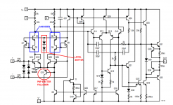
Just like the LT1001 "precision" opamp shown below
_
Just like the LT1001 "precision" opamp shown below
_
Attachments
This is very true, and it is always wise to buffer the tail before using it to drive the bases or gates of cascodes. A P-channel JFET source follower feeding a level shifter is possibly even a better choice. It is also true that the driven cascode I described can't really be applied to a general purpose op amp.
In the case of a buffer on the tail, it is not merely the static base current of a BJT buffer that I worry about. It is possible distortion and CMRR degradation that I worry about. I would point out that the nonlinear collector-base capacitance of the PNP buffer transistor is not bootstrapped out. Maybe I am too obsessed with not screwing with the tail of the input stage. I often cascode the tail current source as well. Finally, I usually place a resistor in series with the tail, often 4.7k or more, to isolate the tail from capacitance. At very high frequencies capacitance on the tail can degrade the LTP's immunity to RFI and increase the chance of rectification at the base-emitter junction of the BJT LTP.
Cheers,
Bob
Neat idea. What is their Vgs at 2 mA?
Do you try to match them? Vgs can be all over the place for MOSFETs, and if their Vgs is too far apart, the input JFETs will see different drain voltages.
Cheers,
Bob
Curiously I have never seen an issue with matching of the mosfets. Usually I get around 3V S-D on the Jfets with the arrangement running the Jfets at 5 mA each. This also minimizes the input capacitance and cap variation with voltage. However I'll be the first to admit you can end up with a VHF oscillator if you aren't careful.
Good point about oscillation. In some way, "bootstrapping" is a euphemism for positive feedback.
Cheers,
Bob
Cheers,
Bob
This is very true, and it is always wise to buffer the tail before using it to drive the bases or gates of cascodes. A P-channel JFET source follower feeding a level shifter is possibly even a better choice. It is also true that the driven cascode I described can't really be applied to a general purpose op amp.
The driven cascode is really an archaic circuit from the days where transistors were expensive. Nowadays, the circuit that Mark shows is much superior. All precision op-amps pretty much use a similar scheme.
To be more precise, the scheme used in the LT0001 was abandoned many years ago. Q3 and Q4 are actually not cascodes, they are current sampling transistors that are used to cancel the base current of the input transistors Q1 and Q2. Q5 and Q6 actually both serve as a cascode and equalizes the VCE of Q1/Q2 and Q3/Q4. The problem of this scheme though is headroom, it eats a VBE worth.
Nowadays you just cascode once (do away with Q3/4, Q7/8) and inject 2 laser trimmed currents into the bases of Q1 and Q2 to achieve perfect cancellation.
A P-channel JFET source follower feeding a level shifter is possibly even a better choice.
Buys you very little unless you have PNPs with miserable Betas. If PNP Beta is 50 or better (not a high hurdle), do not bother with JFETS.
In the case of a buffer on the tail, it is not merely the static base current of a BJT buffer that I worry about. It is possible distortion and CMRR degradation that I worry about. I would point out that the nonlinear collector-base capacitance of the PNP buffer transistor is not bootstrapped out.
True, capacitance in the common node of the LTP will give higher 2nd harmonics, but decent discrete PNPs have CJC's of 2pF or so. Too low to matter in the audio frequency.
Maybe I am too obsessed with not screwing with the tail of the input stage. I often cascode the tail current source as well. Finally, I usually place a resistor in series with the tail, often 4.7k or more, to isolate the tail from capacitance. At very high frequencies capacitance on the tail can degrade the LTP's immunity to RFI and increase the chance of rectification at the base-emitter junction of the BJT LTP.
Yes you are Bob. Itail is not such a big deal since errors there are common mode. I would be more worried about not screwing up the current mirror whose errors are differential mode. The RFI is probably a valid point, but if you have a good RFI filter in the input network, then it is really diminishing returns.
Cheers!
The driven cascode as I described it (cascode gates or bases driven from an output-derived replica of the feedback signal) is indeed old - I employed in the 80's in a refinement of my MOSFET power amplifier with error correction, and it further reduced distortion. Those were not the days of expensive transistors - that is totally not the issue. As I stated above, the driven cascode is not applicable to op amps. Maybe you overlooked that point.
Can you cite an example of where the driven cascode as I described it was used in a power amplifier?
Also, for the application to a power amplifier, can you explain why circuits using a derived signal from the tail are superior in this application?
Cheers,
Bob
Can you cite an example of where the driven cascode as I described it was used in a power amplifier?
Also, for the application to a power amplifier, can you explain why circuits using a derived signal from the tail are superior in this application?
Cheers,
Bob
Hi Bob,
1. Due to the large voltage at the output of the amp, you need a voltage divider using medium size resistor values to keep the power dissipation low. Hence you have a sizable impedance at the base of the cascode. This impedance interacts with the base current of the cascode which will give modulate their emitter voltages and hence inject current through the CJC of the input transistors to the FB and input networks. This may give you distortion. Measurement to be done to verify.
2. Using the "derived signal from the tail" circuit, if you are clever, you can recycle the base current of the cascode to eliminate the Beta distortion introduced by the cascode. If you use JFETs and MOSFETS for cascoding, this is not an issue.
I'll think of a few more, but these are the first things that come mind.
Unless it is a fixed gain op-amp. Gain of 2 op-amps were very popular for video applications. PGA's at gains of 1,2,5,10 are very popular for data acquisition. I used the scheme in a Brokaw cell type reference. Sadly, I had to remove it because under certain conditions it latched... long story on why it did that.As I stated above, the driven cascode is not applicable to op amps
My explanation on the LT1001 scheme, why it is out of date, and what is used now, only applies to op-amps... so not overlooked. It also applies to In-amps.Maybe you overlooked that point.
Yes, your own paper. 🙂Can you cite an example of where the driven cascode as I described it was used in a power amplifier?
Remember I am coming from the perspective of how we do things in op-amps, but here are a couple of ideas...Also, for the application to a power amplifier, can you explain why circuits using a derived signal from the tail are superior in this application?
1. Due to the large voltage at the output of the amp, you need a voltage divider using medium size resistor values to keep the power dissipation low. Hence you have a sizable impedance at the base of the cascode. This impedance interacts with the base current of the cascode which will give modulate their emitter voltages and hence inject current through the CJC of the input transistors to the FB and input networks. This may give you distortion. Measurement to be done to verify.
2. Using the "derived signal from the tail" circuit, if you are clever, you can recycle the base current of the cascode to eliminate the Beta distortion introduced by the cascode. If you use JFETs and MOSFETS for cascoding, this is not an issue.
I'll think of a few more, but these are the first things that come mind.
Sounds like we are largely in agreement as long as the context is clear, i.e., op amps vs discrete power amps, etc.
Things like this usually boil down to design preferences that are based on one's own experience and one's priorities on inevitable engineering tradeoffs. There are many, many judgment calls in engineering. The tail-driven cascode, when properly implemented with a buffer and adequate amount of level shifting, is perfectly satisfactory.
Another example of such tradeoffs and judgement calls is whether to use BJTs or JFETs in the input LTP. My preference always leans to JFETs, but many will argue differently. Many wonderful amplifiers have been implemented with BJT input LTPs (probably many more than with JFETs), but I think the tradeoffs favor JFETs (which are inevitably more expensive when in the form of dual monolithic pairs).
Discussions like this help educate the readers (and the writers!) and provide insight, regardless of which approach the reader ends up choosing.
Cheers,
Bob
Cheers,
Bob
JFETs vs BJT inputs... that is an interesting call.
In op-amps JFET input is considered specialty since their noise, offset, input capacitance is higher and mostly only customers looking for ultra low input bias current would consider them.
For power amps, I have not made my mind yet. If gunning for the lowest distortion numbers at every gain stage of the amp, BJT's are probably the way to go. But, if I were to be subjective (I am not), I could argue that the x^2 I/V transfer of the JFET has a more pleasing distortion (whatever that means).
So... I don't have a stance on it yet. Given the choice, I would probably go for BJT only because there are more of them to choose from... but again is not a strong/well argued preference.
Best, Sandro
Hi Jerome,
I am completely fine with posting a scan of a page from my book. It helps everyone understand the post, especially those who don't have a copy of my book.
The quasi-differential input can be thought of as follows. Consider the classic single op-amp differential amplifier with four equal resistors; R1 to the negative input, R2 to the positive input, R3 from output to negative input; R4 from positive input to ground.
Note that R2 merely provides the overall positive signal input to the op amp positive input through some attenuation.
Now think of the core of the power amplifier as an op amp. The main feedback resistor corresponds to R3 and the feedback shunt resistor corresponds to R1. The series input resistance corresponds to R2 and the subsequent shunt resistance corresponds to R4. We have an approximation of the classic single op amp differential amplifier, in which "R1", the inverting input, is connected to the shield of the amplifier input jack.
The resistors are not all equal, as the gain is set to be about 28, as determined by the ratio of "R3" to "R1". Moreover, the actual values of "R2" and "R4" need not be the same as "R3" and "R1" as long as their ratio is appropriate for differential amplifier operation with some common mode rejection. The common mode rejection of this arrangement is, of course, degraded by the source impedance of the preamplifier.
Cheers,
Bob
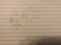
Hi Bob,
I don't really "see" the differential output amplifier. Is this schematic correct?
Attachments
Yes, it is an interesting call for a power amplifier, involving many tradeoffs, the weight put on each tradeoff, and the context of the circuit. I've built many amplifiers with both, and both types measure well. Distortion in every amplifier I have made has been dominated by the output stage rather than the IPS/VAS (and is still quite low).
In fact, without special measures like error correction, lateral or vertical output stages tend to contribute numerically more distortion, but the nature of the distortion tends to be somewhat different. There are those who prefer a MOSFET output over a BJT output in spite of the fact that the MOSFET might have numerically higher distortion. One reason may be that you can bias MOSFET output at much higher current than BJTs without risking GM-doubling distortion. I know that talking about BJT vs MOSFET outputs is a bit off-topic for this post, but it helps to show an example of how complex these tradeoffs can be.
Notably, Erno Borbely strongly preferred JFET input stages as do many notable high-end audiophile designers.
RFI susceptibility can be complex and controversial, but it is quite clear that JFETs are more immune, since the input signal is being applied to a reverse-biased junction instead of a forward-biased junction. While HF filtering at the input of an amplifier is common, implementations vary widely and some are more effective than others.
The issue of input offset can go either way depending on the amplifier's circuit design and design priorities. While a dual monolithic JFET may have offset of +/- 10 mV, and a matched BJT input pair may have only +/- 1 mV offset (or far less), the input bias current of a BJT can create significantly more offset than the JFET unless the BJT beta is very high. Consider an ordinary BJT with beta of 100 and biased at 1 mA. Input bias current will be 1.0 uA - seems like not much. But what if you want to have fairly high amplifier input impedance so you can use a quality input coupling capacitor that is not huge and expensive. Suppose you pick a 100k return resistor. The BJT will cause 100 mV of offset, 10 times that of the JFET. Although there are tricks to mitigate the issue, the JFET frees you up from having the feedback resistor at almost the same value as the input return resistor in an attempt to cancel input-bias-current-induced offset voltage. For the sake of noise, you really want to be free to use a fairly low impedance feedback network. I usually like to use a DC servo anyway.
Cheers,
Bob
In his last series of all fet power amps Erno also used a jfet cascode for the VAS using matched quad of parralled 2SK170/2SJ74 each with idss above 8 ma so the VAS current was 16 ma. The cascode devices were the 2SK2013/2SJ313 Fets. It was differentially driven as Erno credited Lender for the differential to single ended conversion idea.
The fet output stage was driven by 2SK216/2SJ79 driver fets
Even the regulators for the front end were all discrete jfet/fet designs and used the dual package 2SK389/2SJ109 cascoded there as well. When using Hitachi laterals even the bias spreader was a 2SK216 fet. Just about every jfet and fet in the design is discontinued unfortunately. The feedback resistor was a 2k TO220 power film.
Attachments
Last edited:
I found that latfet can use in simple circuit. Although the distortion is high, but sound pleasing to many people. But I can not use it same way for BJT.
I think amplifier designer must consider human perception. The goal is not only high linearity, but can also sound pleasing. Example: guitar amplifier. Or cheap but sound pleasing 🙂
I think amplifier designer must consider human perception. The goal is not only high linearity, but can also sound pleasing. Example: guitar amplifier. Or cheap but sound pleasing 🙂
I actually completely disagree with that.
Guitar amplifiers are not HiFi amplifiers, they are guitar amplifier. Electric guitars have no sound, since they don't have an acoustic box like an acoustic guitar (try to play one without an amp). As a result, a guitar amp is an integral part of the sound of an electric guitar, i.e. the amp has 2 roles: amplify + provide a guitar sound effect. In more engineering terms, the electric guitar amplifier needs to distort to give the guitar a spefic sound. That is why there is no successful linear guitar amp in the market. BTW, the sound of guitar amps have nothing to do with human perception, it is the sound we associate with electric guitars, just like the sound associated with drums, and all other instruments. Another way to say is, the electric guitar by itself is not really an instrument, it is the guitar + its guitar amp.
Now, let's turn to hifi amps. Human perception changes from person to person, so designing for it is a loosing proposition. Worse yet, designing for 'sounds good' is subjectivist nonsense. What is true is that ultra high levels of linearity is not necessary to be a good amp. Most people can't tell the difference after day 0.01% THD. Those who can are either exceptional or exceptional liars. I don't think I can tell the difference between 0.1% or better [my hearing is terrible]. Ian Heglum has quite a few references that have convinced me that most properly designed HIFI amps sound about the same provided they are not clipping.
Now, if you want to brag about how good your amp is, design for ultra low distortion. It may not make much of difference in hearing due to what I said in the previous paragraph, but at least you can say my amp distorts less than yours, and you can measure it. If you want to incorporate human perception, get a nice sound processor that can twist the signal in a million ways, stick it before your pre-amp, and program it until you find the sound you like. Also you can use it to compensate for room accoustics, the speaker, etc. Furthermore, if you say a sound processor cannot immitate the sound of say 'tubes', then get a tube pre-amp (problem solved).
Hi Bob,
I don't really "see" the differential output amplifier. Is this schematic correct?
See the attached picture...
Attachments
In his last series of all fet power amps Erno also used a jfet cascode for the VAS using matched quad of parralled 2SK170/2SJ74 each with idss above 8 ma so the VAS current was 16 ma. The cascode devices were the 2SK2013/2SJ313 Fets. It was differentially driven as Erno credited Lender for the differential to single ended conversion idea.
The fet output stage was driven by 2SK216/2SJ79 driver fets
Even the regulators for the front end were all discrete jfet/fet designs and used the dual package 2SK389/2SJ109 cascoded there as well. When using Hitachi laterals even the bias spreader was a 2SK216 fet. Just about every jfet and fet in the design is discontinued unfortunately. The feedback resistor was a 2k TO220 power film.
Yes, Erno Borbely did some great work, and was a pioneer in advocating the use of JFETs and MOSFETs in power amplifiers.
I should point out that the 2SK170, 2SJ74 and 2SK389 are available from Linear Integrated Systems (LIS) as the LSK170, LSJ74 and LSK389. I am very familiar with these parts and they have excellent performance.
The LSK489 and LSJ689 are also available as a complementary pair. These devices have a bit smaller geometry than the LSK389 and a bit higher noise and notably smaller capacitance. While the LSK389 is capable of 1 nV/rt for each device in the dual, the LSK489 and LSJ689 are closer to the 2 nV/rt Hz range, still very capable of implementing a very low noise power amplifier. These are the devices that I used in the DH-220C amplifier (Hafler DH220 upgrade) described in my second edition and for which PCBs are available.
Cheers,
Bob
- Home
- Amplifiers
- Solid State
- Bob Cordell's Power amplifier book