Why Q3 could saturate? Bob writes :" when negative clipping occurs, the IPS output will try to turn on the VAS transistor harder". I am OK with that, when negative clipping occurs, Q1 conduct more, so Q11 and Q12 as well, and Q12 could saturate. If Q12 is in saturation, voltage at the base of Q11 is very low and Q11 and Q12 couldn't conduct anymore. Is this reasoning incorrect?
"when negative clipping occurs, the IPS output will try to turn on the VAS transistor harder".
Are you sure, this is what it says? If it is, it is wrong.
When POSITIVE clipping occurs, the IPS will try to turn on the VAS transistor harder. This way, the VAS transistor will try to pull the output down. The VAS stage is inverting, so turning it ON more, pulls down.
When postive clipping occurs, Q1 base is lower than Q2 base, Q1 conducts more, current is injected to base of Q11 which turns the VAS ON more.
When the negative clipping occurs, Q2 base is lower than Q1, Q2 conducts more, the mirror mirror conducts more such that |IC_Q3| > |IC_Q1|, the base of Q11 is pulled down, the VAS turns off, bringing the collector voltage of Q3 very low and saturating the transistor... unless D6 is present. D6 will hold the collector of voltage of Q3 at VEE+~1V. This one volt is not enough to keep the VAS on (you need 2VBE = ~1.4V), but at least Q3 won't saturate.
makes sense?
I am sure about that, but there is something strange in your explanation. When negative clipping occurs, in my opinion, it means, when there is a negative signal at the input. So, when a negative clipping occurs Q1 base is lower than Q2 base, Q1 conducts more and Q11 turns the VAS more, this explanation seems correct, isn'it. Bob writes "when negative clipping occurs, the input of Q11 increases" On the other, when a positive clipping ocurs, Q2 conducts more, and by this way Q3 could come in saturation, unless D6 is present.
Hi Jerome, it looks like when I transcribed the circuit to a piece of paper to do a quick analysis, I messed up the labels and got them backwards. Here it is again, now I am being super careful...
Postive clipping:
- Q1 base > Q2 base => Q2 conducts tail current
- The current mirror conducts more such that |IC_Q3| > |IC_Q1|
- The base of Q11 is pulled down, the VAS turns off, bringing the collector voltage of Q3 very low and saturating the transistor... unless D6 is present
- D6 will hold the collector of voltage of Q3 at VEE+~1V. This one volt is not enough to keep the VAS on (you need 2VBE = ~1.4V), but at least Q3 won't saturate.
- VAS off means the second stage pulls the output high causing positive clipping.
Negative clipping:
- Q1 base < Q2 base => Q1 conducts tail current
- Q1 current is injected to base of Q11 which turns the VAS ON more.
- VAS very ON pulls the output further negative to negative clipping.
Anyway, back to the original question, D6 helps recovery on Positive clipping by preventing Q3 from saturating.
Hope this helps,
Best, Sandro
I don't understand the interest of anti-parallel D5 and D6. Could you explain the goal of these diodes? This is in page 89
The nominal voltage at the collector of Q3, driving the 2T VAS, is about 1.4V (roughly 2 Vbe + the drop across R21). If you assume that the forward on voltage of D5 and D6 is 1 Vbe (it tends to be a bit less), then the anti-parallel diodes prevent the drive to the VAS from being more than 1 Vbe away from the nominal voltage in either direction when there is clipping.
Importantly, this limits the positive over-voltage drive to the VAS when there is negative clipping at the amplifier output. This is the primary function of D5. D6 turns on when there is positive clipping at the output of the amplifier, and it prevents Q3 from saturating.
Cheers,
Bob
"when negative clipping occurs, the IPS output will try to turn on the VAS transistor harder".
Are you sure, this is what it says? If it is, it is wrong.
When POSITIVE clipping occurs, the IPS will try to turn on the VAS transistor harder. This way, the VAS transistor will try to pull the output down. The VAS stage is inverting, so turning it ON more, pulls down.
When postive clipping occurs, Q1 base is lower than Q2 base, Q1 conducts more, current is injected to base of Q11 which turns the VAS ON more.
When the negative clipping occurs, Q2 base is lower than Q1, Q2 conducts more, the mirror mirror conducts more such that |IC_Q3| > |IC_Q1|, the base of Q11 is pulled down, the VAS turns off, bringing the collector voltage of Q3 very low and saturating the transistor... unless D6 is present. D6 will hold the collector of voltage of Q3 at VEE+~1V. This one volt is not enough to keep the VAS on (you need 2VBE = ~1.4V), but at least Q3 won't saturate.
makes sense?
"when negative clipping occurs, the IPS output will try to turn on the VAS transistor harder" is correct. When the amplifier output clips negative, that means that the output cannot go as negative as it should. The VAS transistor, in turning on, tries to pull the output more negative, but to no avail. Thus, the IPS tries to turn on the VAS transistor harder.
Under conditions of negative clipping, IPS transistor Q1 turns on hard (the input is going negative and Q1 is a PNP). As Q1 turns on hard, the collector voltage of Q3 rises, turning on the VAS transistor hard. D5 conducts, limiting this turn-on voltage and in turn helps limit the current in VAS EF transistor Q11, helping to keep it in its safe area; Q11 has nearly the negative rail voltage across it. VAS transistor Q12 will still saturate under these conditions, and its turn-off time from saturation can be a concern under some high-frequency laboratory testing conditions that will never occur in normal audio signal processing (prolonged sinewave clipping at ultrasonic frequencies).
Cheers,
Bob
 Thank you to both of you. I have another question, in the same chapter, I don't know the interest of R6, R5 and R4. Ok R4 is there to avoid ground loops, Ok for that, but when Bob writes "This arrangement, in combination with the small signal attenuation of R4 against R5, gives the amplifier some of the properties of a differential input". I don't see a "kind" of differential input for these parts
Don't want to be the party pooper here but isn't it copyright infringment to scan the pages and upload them that way? I know that its for educational purposes and if Bob, the author, is ok with it then there shouldn't be a problem, Bob seems like a really nice guy to say something so I will.
I would advice jerome86 that instead of uploading an image, that he refers to the part and page numbers without uploading a photo of the text.
I would advice jerome86 that instead of uploading an image, that he refers to the part and page numbers without uploading a photo of the text.
Last edited:
These diodes are almost exactly what I did to "fix" Yamaha P2200 amps back in the 1980s. Used by bands for the high end horns, this amp produced a nasty spike, particularly on the positive overload recovery (aka rail sticking) that damaged horns. Perhaps unlike home stereo, bands clip their amps constantly. The log nature of hearing means that they always turn it up until it clips no mater how much power they have.
At that time, we also sold Spectrosonic modular amps which were dogs for slew rate but had zero rail sticking, which meant a limited amount of clipping was barely noticeable and many people loved the sound.
So, especially for professional use, clipping behavior is very important. This is not unrelated to the idea that pro sound requires using amps that are not large enough to damage the connected speakers. Pro sound is always tri-amp'd (or more) so clipping harmonics are naturally attenuated by the (bass, mid) speaker HF roll off. The horns being relatively efficient meant the high end amp was the last to clip and at a painful level that the lower drivers could not match.
Last edited:
I've made some simulations with and without the diodes, the diodes do seem to increase THD ever so slightly.
I could understand, but the two last pictures sent are available on internet.
404 Not Found
So I'm not sure that the picture sent is a problem, Bob could you confirm taht?
404 Not Found
So I'm not sure that the picture sent is a problem, Bob could you confirm taht?
View attachment 862821Thank you to both of you. I have another question, in the same chapter, I don't know the interest of R6, R5 and R4. Ok R4 is there to avoid ground loops, Ok for that, but when Bob writes "This arrangement, in combination with the small signal attenuation of R4 against R5, gives the amplifier some of the properties of a differential input". I don't see a "kind" of differential input for these parts
Hi Jerome,
I am completely fine with posting a scan of a page from my book. It helps everyone understand the post, especially those who don't have a copy of my book.
The quasi-differential input can be thought of as follows. Consider the classic single op-amp differential amplifier with four equal resistors; R1 to the negative input, R2 to the positive input, R3 from output to negative input; R4 from positive input to ground.
Note that R2 merely provides the overall positive signal input to the op amp positive input through some attenuation.
Now think of the core of the power amplifier as an op amp. The main feedback resistor corresponds to R3 and the feedback shunt resistor corresponds to R1. The series input resistance corresponds to R2 and the subsequent shunt resistance corresponds to R4. We have an approximation of the classic single op amp differential amplifier, in which "R1", the inverting input, is connected to the shield of the amplifier input jack.
The resistors are not all equal, as the gain is set to be about 28, as determined by the ratio of "R3" to "R1". Moreover, the actual values of "R2" and "R4" need not be the same as "R3" and "R1" as long as their ratio is appropriate for differential amplifier operation with some common mode rejection. The common mode rejection of this arrangement is, of course, degraded by the source impedance of the preamplifier.
Cheers,
Bob
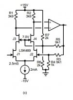
Driven Cascode
Hi Bob,
Question on the driven cascode from your LSK489 application note paper. With this circuit can the cascode devices J3 & J4 be the same type as the input devices J1 & J2? Or do they need need to be higher Vp rated devices?
Erno Borbely makes this case in his JFETs: The New Frontier, Part 1 article so I assume that's the case.
If this is the case, do you have any recommendations for leaded devices for cascoding the LSK170? I believe the devices Borbely identified are no longer available.
Hi Bob,
Question on the driven cascode from your LSK489 application note paper. With this circuit can the cascode devices J3 & J4 be the same type as the input devices J1 & J2? Or do they need need to be higher Vp rated devices?
Erno Borbely makes this case in his JFETs: The New Frontier, Part 1 article so I assume that's the case.
Erno Borbely said:I am using a high-VP JFET for the upper device, so that the lower JFET has enough voltage across it to operate in the saturation region.
If this is the case, do you have any recommendations for leaded devices for cascoding the LSK170? I believe the devices Borbely identified are no longer available.
Attachments
Hi Brian,
The cascode JFETs in the driven cascode can be the same type as those used below, and need not be high Vp devices. This is because the driven cascode approach provides a positive bias voltage for the gates of the cascode transistors. Other approaches, where the gate of the cascode is biased from the source of the device below, do indeed work better with a high-Vp device for the cascode device. Of course, the cascode transistors in the driven cascode can just as well be implemented with BJTs.
BTW, I fully agree with what Erno said about his preference for using JFETs, especially in the input stage. We both like JFET-BJT-MOSFET topologies.
Cheers,
Bob
So the cascode device can be a BJT and achieve the same result of reducing the input capacitance of the input JFETs?
Your paper indicates that using JFETs for the cascode can reduce noise from the cascode, but it sounds like you prefer BJTs for the cascode in this arrangement. Do I have that correct?
Your paper indicates that using JFETs for the cascode can reduce noise from the cascode, but it sounds like you prefer BJTs for the cascode in this arrangement. Do I have that correct?
Yes, BJT's can be used for the cascode. However, it is true that there is a rather slight noise advantage with JFETs in the cascode because there is no base current to contribute to the noise. With a JFET cascode virtually ALL of the signal current from below into the source ends up at the drain.
Incidentally, BJTs usually are available with significantly higher voltage ratings than JFETs, the latter often available with only a 40-V or so rating. If you use JFETs in the input stage of a conventional Thompson power amplifier that has high rail voltages of, say 65 V, you will likely need BJT cascodes to cope with the higher rail voltage. As an example, it is common to bias the BJT cascode bases at +15 V, in which case the BJT cascodes would have on the order of 48-50 V across them with a 65 V rail.
Cheers,
Bob
Thanks for the explanations and quick reply. Your patience for our myriad of questions seems endless. And to test that a bit further...
If JFETS are used and are of the same type as the input devices, is there any need to match the on Idss? I assume only the cascode devices themselves should be matched and that there's no need to match the cascode to the input.
If JFETS are used and are of the same type as the input devices, is there any need to match the on Idss? I assume only the cascode devices themselves should be matched and that there's no need to match the cascode to the input.
- Home
- Amplifiers
- Solid State
- Bob Cordell's Power amplifier book