Samuel Groner proposed this scheme.Bob, what about using jfet as a helper transistor in current mirror? Perhaps it takes a LED or something similar in series with source to get proper voltages. It would certainly improve the speed and linearity, plus the value of the third (non degenerative) resistor would be much less critical.
Attachments
This sort of thing is one of the reasons I wanted to put anti-polarity clamp diodes across the IPS collectors, so as to limit the voltage swing in clipping to no more than +/- one Vbe about the nominal voltage. One concern in the 2T VAS is over-current in the EF transistor when it tries to drive the emitter of the saturated VAS transistor through its base. There can even be a safe area concern for that EF transistor. With the positive swing out of the mirror limited to no more than 1Vbe above nominal, the amount of this over-current is easier to control. In my design, I place a 50-ohm resistor between the emitter of the emitter follower and the base of the VAS transistor. This, in combination with the typical 22-ohm VAS transistor emitter degeneration helps limit the current in the EF transistor during clipping.
Cheers,
Bob
It's easy to limit VAS overdrive by placing protecting resistor in the EF transistor collector.
BR Damir

😉
Why do you think this? "isn't even close" is a bold claim.
I have looked at this both mathematically and in simulation, and I found the noise reduction much past 260 mV is small.
The exact reduction depends on the circuit, typically the reduction possible is in the order of a dB, hardly dramatic to improve the S/N from, say, 110 dB to 111.
Toni (ASTX) and I discussed this in the thread to which he provided a link.
In the early part of that thread I comment that I tried up to 2.6 V, with asymptotically smaller improvement.
So Keantoken's advice of 300 mV and Bob's of 234 mV seem not unreasonable to me.
Of course, even a "free" dB is nice so Toni increased it until other issues occurred.
He arrived at 600 mV, still reasonable.
My advice was to the OP, who is probably better off with a more conventional circuit rather than an extreme attempt to push the limit, even if Toni and I had fun to find small improvements.😉
Best wishes
David
...I think... drop of a few 100 mV in CCS and CM isn't even close to what is needed...
Why do you think this? "isn't even close" is a bold claim.
I have looked at this both mathematically and in simulation, and I found the noise reduction much past 260 mV is small.
The exact reduction depends on the circuit, typically the reduction possible is in the order of a dB, hardly dramatic to improve the S/N from, say, 110 dB to 111.
Toni (ASTX) and I discussed this in the thread to which he provided a link.
In the early part of that thread I comment that I tried up to 2.6 V, with asymptotically smaller improvement.
So Keantoken's advice of 300 mV and Bob's of 234 mV seem not unreasonable to me.
Of course, even a "free" dB is nice so Toni increased it until other issues occurred.
He arrived at 600 mV, still reasonable.
My advice was to the OP, who is probably better off with a more conventional circuit rather than an extreme attempt to push the limit, even if Toni and I had fun to find small improvements.😉
Best wishes
David
Last edited:
This is what I had in mind (but no adequate drawing SW at hand 🙂 )
Funny thing is that one is one of the oldest SW man kind invented along with the constant upgrades and no bugs...ever!🙂
Modulation of noise floor?
Hi All,
since there has been some discussion about noise performance on the last pages, I'd like to pose a question.
The noise density generated by circuit elements is normally considered as fixed, perhaps a bit depending on operating point if stemming from active devices. Is it possible -- in principle and in practice -- that the noise spectrum is modulated by the signal? Then, it would not be anymore "real noise".
Kind regards,
Matthias
...
Of course, even a "free" dB is nice so Toni increased it until other issues occurred.
He arrived at 600 mV, still reasonable.
...
On all 5 pics SA2016 IXYS VMOS amp modules I have used transistors without any matching. Only checked with DCA75 if in good working condition.
The 600mV tolerance in current mirror helps here too.
All 5 modules have excellent measurement results. 🙂
BR, Toni
It's easy to limit VAS overdrive by placing protecting resistor in the EF transistor collector.
BR Damir
This is true, but consider the size of that resistor and the effect the resulting signal at the collector will have on circuit performance unless that collector is ac-bypassed. If the rails are 50V and the collector is connected to ground, and we wish to limit max current to 10mA, the resistor must be about 5k. That would permit significant signal there, depending on signal drive current for the VAS transistor, including that required to drive Ccb of that transistor. The signal at the collector of the EF would then come back to the EF base via its Ccb and Early effect. Thus, at minimum, we would have to bypass that collector, which would then permit high current for small intervals. This approach thus has its own issues.
Cheers,
Bob
This is what I had in mind (but no adequate drawing SW at hand 🙂 )
That should work, but I'm not sure it is an improvement at the end of the day, and it does not equalize mirror collector voltages.
Cheers,
Bob
Hi All,
since there has been some discussion about noise performance on the last pages, I'd like to pose a question.
The noise density generated by circuit elements is normally considered as fixed, perhaps a bit depending on operating point if stemming from active devices. Is it possible -- in principle and in practice -- that the noise spectrum is modulated by the signal? Then, it would not be anymore "real noise".
Kind regards,
Matthias
Virtually any aspect of performance of an amplifier can be modulated by the instantaneous operating point - this is actually a fundamental cause for distortion. However, in the case of noise I would expect that variation to be quite small. It might originate, for example, from signal current changing the gm of transistors, which can influence the noise they contribute. But the effect should be very small.
Cheers,
Bob
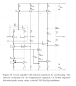
Samuel Groner proposed this scheme.
So did I:
... redeploy the original 741 opamp's current mirror load, but replace bipolar emitter followers Q7 and Q16, with MOSFET source followers M1 and M2. Be sure to match the MOSFET load resistors R1 and R2, just as Fullagar matched the 50K emitter load resistors in the 741. We're not building a low power opamp so we can use source leg resistors a lot lower than 50K! Fortunately we can buy dual MOSFETs whose two devices are manufactured side-by-side on the same wafer, see pdf datasheet attached.
M1 supplies all base current, thus the mirror loads are not unbalanced. M1+M2 ensure the mirror collector voltages are balanced. The high input impedance of M1+M2 increases the low frequency gain (Zload / gm) of the IPS. What's not to like?
So did I:
M1 supplies all base current, thus the mirror loads are not unbalanced. M1+M2 ensure the mirror collector voltages are balanced. The high input impedance of M1+M2 increases the low frequency gain (Zload / gm) of the IPS. What's not to like?
M1 and M2 need to be matched. That's kind of not to like.
Cheers,
Bob
So did I:
M1 supplies all base current, thus the mirror loads are not unbalanced. M1+M2 ensure the mirror collector voltages are balanced. The high input impedance of M1+M2 increases the low frequency gain (Zload / gm) of the IPS. What's not to like?
If M1 and M2 are N-channel JFETs, their sources need to be positive wrt to their gates. That would force the BJT VCE to zero or very small, I think.
Cheers,
Bob
This is true, but consider the size of that resistor and the effect the resulting signal at the collector will have on circuit performance unless that collector is ac-bypassed. If the rails are 50V and the collector is connected to ground, and we wish to limit max current to 10mA, the resistor must be about 5k. That would permit significant signal there, depending on signal drive current for the VAS transistor, including that required to drive Ccb of that transistor. The signal at the collector of the EF would then come back to the EF base via its Ccb and Early effect. Thus, at minimum, we would have to bypass that collector, which would then permit high current for small intervals. This approach thus has its own issues.
Cheers,
Bob
I don't think that resistor is a problem and not need to be bypassed, at least it's only EF and collector voltage fluctuation, even with 5k resistor, is very low even at full power. Distortion simulation at full power with and without protection resistor shows no difference at 1 kHz and only very small increase at 20 kHz. In case of VFA with JFET LTP I used 4k7 resistor and I case of CFA I used 6k8 resistors. Built CFA distortion measurement shows only 3 to 4 times higher distortion at 20 kHz at full power then simulated. (simulated THD20 at 200W/8 was 3.6 ppm and measured just 3 to 4 times higher, on all account very low).
By the way Bob have you included in your new book edition any example and analysis of an amp with symmetric complementary IPS or CFA?
Best wishes, Damir
M1 and M2 need to be matched. That's kind of not to like.
Did you see this part of the same posting
Fortunately we can buy dual MOSFETs whose two devices are manufactured side-by-side on the same wafer, see pdf datasheet attached.
But perhaps the biggest concern isn't matching between M1 and M2; rather it's repeatability of the threshold voltage of M2 when you build five thousand amplifiers with five thousand M2 devices. If/when M2's threshold varies from amplifier to amplifier, the input bias point of the VAS changes, which requires DC NFB to introduce an output offset that moves the VAS back into balance. Ick. Looks pretty on the schematic though.
Attachments
Last edited:
If M1 and M2 are N-channel JFETs, their sources need to be positive wrt to their gates. That would force the BJT VCE to zero or very small, I think.
Cheers,
Bob
Use P JET's it looks strange but it works. The sources are pulled up to the + rail and the drains to the - rail.
And double up the pjfet with Mark's need for matched M1 and M2 by paralleling undersized ones (and thus statistically getting tighter control without matching) 😀
M1 and M2 need to be matched
Suppose we use them anyway even though they are NOT matched. Suppose their gate threshold voltage "VTH" values are 1000 millivolts apart.
Then the Perfectly Balanced point for the current mirror, would have the collector voltages 1000 millivolts apart. Let's figure out what it will take to get those collector voltages back to equal.
Using the Cordell Audio spice model of the 2N5551 transistor, I simulated a 3T current mirror with emitter degeneration resistors equal to 9 * (1/gm of the mirror devices). Running at 2mA per side, Spice said the mirror's dynamic output resistance was about 3E+6 ohms.
Thus to pull the mirror back into a condition where the two collectors are the same voltage, we use Ohm's Law to compute the required extra current in one leg of the mirror
- Iextra = 1000mV / 3E+6 ohms
But wait! 0.33uA is 0.017% of the per-leg mirror current. The emitter degeneration resistors are ±1% (or maybe ±0.1% if you're xnal-retentive). So the mismatch in M1-M2 is completely negligible compared to the mismatch in 3TCS emitter degeneration resistor. And NOBODY worries about mismatch in degeneration resistors. I checked Bob Cordell's JAES amplifier paper: no mention of mismatch in degeneration resistors. I checked Bob Cordell's book, Chapter 7: no mention of mismatch in degeneration resistors.
And yet a quick simulation verifies what intuition predicts: a 1% mismatch in current mirror degeneration resistors, gives a 1% mismatch in currents between left-leg and right-leg.
So it seems that M1-M2 mismatch is a much smaller contributor to current mirror imbalence, than emitter degeneration resistor mismatch. What a pleasant result.
Did you see this part of the same posting
But perhaps the biggest concern isn't matching between M1 and M2; rather it's repeatability of the threshold voltage of M2 when you build five thousand amplifiers with five thousand M2 devices. If/when M2's threshold varies from amplifier to amplifier, the input bias point of the VAS changes, which requires DC NFB to introduce an output offset that moves the VAS back into balance. Ick. Looks pretty on the schematic though.
Sorry, I didn't realize you were suggesting MOSFETs.
Bob
Suppose we use them anyway even though they are NOT matched. Suppose their gate threshold voltage "VTH" values are 1000 millivolts apart.
Then the Perfectly Balanced point for the current mirror, would have the collector voltages 1000 millivolts apart. Let's figure out what it will take to get those collector voltages back to equal.
Using the Cordell Audio spice model of the 2N5551 transistor, I simulated a 3T current mirror with emitter degeneration resistors equal to 9 * (1/gm of the mirror devices). Running at 2mA per side, Spice said the mirror's dynamic output resistance was about 3E+6 ohms.
Thus to pull the mirror back into a condition where the two collectors are the same voltage, we use Ohm's Law to compute the required extra current in one leg of the mirror
So Iextra is 0.33 microamperes. That's the "Current mismatch" caused by a 1000mV mismatch in the threshold voltages of M1 and M2.
- Iextra = 1000mV / 3E+6 ohms
But wait! 0.33uA is 0.017% of the per-leg mirror current. The emitter degeneration resistors are ±1% (or maybe ±0.1% if you're xnal-retentive). So the mismatch in M1-M2 is completely negligible compared to the mismatch in 3TCS emitter degeneration resistor. And NOBODY worries about mismatch in degeneration resistors. I checked Bob Cordell's JAES amplifier paper: no mention of mismatch in degeneration resistors. I checked Bob Cordell's book, Chapter 7: no mention of mismatch in degeneration resistors.
And yet a quick simulation verifies what intuition predicts: a 1% mismatch in current mirror degeneration resistors, gives a 1% mismatch in currents between left-leg and right-leg.
So it seems that M1-M2 mismatch is a much smaller contributor to current mirror imbalence, than emitter degeneration resistor mismatch. What a pleasant result.
Good points. I always assume the use of 1% metal film mirror degeneration resistors. If they are in the extreme +1% and -1% each, then the mirror's common mode rejection is only 34dB, even if everything else is perfect and there is no current drawn by the base or gate of the helper device.
I don't take the trouble to measure and match 1% metal film resistor pairs, but I always pick adjacent ones off of a tape. They are usually like peas in a pod (but you can't count on it). Same for transistors.
Cheers,
Bob
- Home
- Amplifiers
- Solid State
- Bob Cordell's Power amplifier book