1k0 to 2k0 is usually sufficient to protect a 625mW device on 50V supply rail.This is true, but consider the size of that resistor and the effect the resulting signal at the collector will have on circuit performance unless that collector is ac-bypassed. If the rails are 50V and the collector is connected to ground, and we wish to limit max current to 10mA, the resistor must be about 5k. ........
Suppose we use them anyway even though they are NOT matched. Suppose their gate threshold voltage "VTH" values are 1000 millivolts apart.
Then the Perfectly Balanced point for the current mirror, would have the collector voltages 1000 millivolts apart. Let's figure out what it will take to get those collector voltages back to equal.
Using the Cordell Audio spice model of the 2N5551 transistor, I simulated a 3T current mirror with emitter degeneration resistors equal to 9 * (1/gm of the mirror devices). Running at 2mA per side, Spice said the mirror's dynamic output resistance was about 3E+6 ohms.
Thus to pull the mirror back into a condition where the two collectors are the same voltage, we use Ohm's Law to compute the required extra current in one leg of the mirror
So Iextra is 0.33 microamperes. That's the "Current mismatch" caused by a 1000mV mismatch in the threshold voltages of M1 and M2.
- Iextra = 1000mV / 3E+6 ohms
But wait! 0.33uA is 0.017% of the per-leg mirror current. The emitter degeneration resistors are ±1% (or maybe ±0.1% if you're xnal-retentive). So the mismatch in M1-M2 is completely negligible compared to the mismatch in 3TCS emitter degeneration resistor. And NOBODY worries about mismatch in degeneration resistors. I checked Bob Cordell's JAES amplifier paper: no mention of mismatch in degeneration resistors. I checked Bob Cordell's book, Chapter 7: no mention of mismatch in degeneration resistors.
And yet a quick simulation verifies what intuition predicts: a 1% mismatch in current mirror degeneration resistors, gives a 1% mismatch in currents between left-leg and right-leg.
So it seems that M1-M2 mismatch is a much smaller contributor to current mirror imbalence, than emitter degeneration resistor mismatch. What a pleasant result.
Where a schematic shows pairs of devices/components that look to be the same, I ALWAYS select.Good points. I always assume the use of 1% metal film mirror degeneration resistors. If they are in the extreme +1% and -1% each, then the mirror's common mode rejection is only 34dB, even if everything else is perfect and there is no current drawn by the base or gate of the helper device.
I don't take the trouble to measure and match 1% metal film resistor pairs, but I always pick adjacent ones off of a tape. They are usually like peas in a pod (but you can't count on it). Same for transistors.
Cheers,
Bob
That probably makes me anal by your definition.
Suppose we use them anyway even though they are NOT matched. Suppose their gate threshold voltage "VTH" values are 1000 millivolts apart.
Difference in Vce voltage of Q3 and Q4 will cause mismatch of their Ccb (which is voltage dependent). Also they will dissipate unequally causing some Vbe disbalance. admittedly, the effect would typically be neglectable.
😉
Why do you think this? "isn't even close" is a bold claim.
I have looked at this both mathematically and in simulation, and I found the noise reduction much past 260 mV is small.
The exact reduction depends on the circuit, typically the reduction possible is in the order of a dB, hardly dramatic to improve the S/N from, say, 110 dB to 111.
Toni (ASTX) and I discussed this in the thread to which he provided a link.
In the early part of that thread I comment that I tried up to 2.6 V, with asymptotically smaller improvement.
So Keantoken's advice of 300 mV and Bob's of 234 mV seem not unreasonable to me.
Of course, even a "free" dB is nice so Toni increased it until other issues occurred.
He arrived at 600 mV, still reasonable.
My advice was to the OP, who is probably better off with a more conventional circuit rather than an extreme attempt to push the limit, even if Toni and I had fun to find small improvements.😉
Best wishes
David
Hi
No it's not a bold claim.
I havnt seen the math formula you ar using, but it is clearly different to what I'm using.
If you and some of your friends have a competition in low noise (and THD) design, I'm not going to enter and ruin that competition.
Maybe you could run a simulation that shows the THD+N at various output level and all the simulation results that I show in the the attached pdf files?
It would be nice.
All the best
Reodor
Attachments
Samuel Groner explored this question in measurements on pages 3 and 4 here:
http://www.nanovolt.ch/resources/power_amplifiers/pdf/audio_power_amp_design_comments.pdf
With 2mA per LTP side, 150R emitter resistors in the chart would correspond to my figure of 300mV degeneration. I can understand why some would use a lower number, I place mine close to the end of significant returns.
So what you're saying must be that he did something wrong that causes the curve to level out after 300mV, and that there is still more to gain.
and that there is still more to gain.
Hi
There is still more to gain.
Maybe you could post the simulated (or measured) results of your amp that I'm asking for in my previous post?
Have fun
Reodor
20Hz-20KHz integrated noise of my amp in simuation is 15.8uVrms. Max output is 32Vrms. 32V/15.8uV=126db SNR at max output.
If I increase the current mirror degeneration to 600mV, noise is 14uVrms, corresponding to 127db SNR at full output.
At this point the 680R feedback shunt resistor is the main contributor to noise, with the current mirror being the second contributor.
So higher degeneration does reduce current mirror noise above 300mV, but only in the current mirror and not the noise contribution from anywhere else.
I always assume the use of 1% metal film mirror degeneration resistors. ... I don't take the trouble to measure and match 1% metal film resistor pairs, but I always pick adjacent ones off of a tape.
Then you get, optimistically, 0.2% matching. You could use unmatched MOSFETs for your CS helper and for the input source follower of your VAS, and their 0.017% impact wouldn't affect the current source imbalance at all. Good to know.
Hi Mark.
Could you please post a small circuit diagram using the jfets with the component part numbers I will give building one ago but ill have to order the jfets first. Thanks again for your interest and input to this topic.
Could you please post a small circuit diagram using the jfets with the component part numbers I will give building one ago but ill have to order the jfets first. Thanks again for your interest and input to this topic.
20Hz-20KHz integrated noise of my amp in simuation is 15.8uVrms. Max output is 32Vrms. 32V/15.8uV=126db SNR at max output.
If I increase the current mirror degeneration to 600mV, noise is 14uVrms, corresponding to 127db SNR at full output.
At this point the 680R feedback shunt resistor is the main contributor to noise, with the current mirror being the second contributor.
So higher degeneration does reduce current mirror noise above 300mV, but only in the current mirror and not the noise contribution from anywhere else.
Note that audio power amplifier S/N is usually referred to 2.83 Vrms, which is 1W at 8 ohms. But no matter how you look at it, 15.8 uV rms is a very good number.
Cheers,
Bob
Others mentioned JFETs but I did not. I am proposing to use MOSFETs for the CS helper and for the input to the VAS. In the schematic of post #8811 I drew the transistors M1 and M2 with an insulated gate (i.e. MOS), I gave them a reference ID beginning with the letter "M" (not "J"), and I included a quote which said "Fortunately we can buy dual MOSFETs".Hi Mark.
Could you please post a small circuit diagram using the jfets with the component part numbers I will give building one ago but ill have to order the jfets first. Thanks again for your interest and input to this topic.
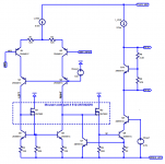
If you are interested in experimenting with a JFET variant, please proceed! But I have no advice or recommendations along those lines. If you are interested in experimenting with the MOSFET version, here is a conceptual circuit schematic that might help you get started:
_
Attachments
Vbias1 = 2V is going to leave Q8 operating with ~ 500 to 550mVcb (or Vce ~ 1100 to 1200mVce)
That is pretty low for a device that is not particularly suited to near saturation.
That is pretty low for a device that is not particularly suited to near saturation.
Thanks Mark. So sorry I did mean MOSFET just didn't double check my post at the time as I have been reading so much lately. Thanks again for your efforts I'll have a closer look when I get home tonight.Others mentioned JFETs but I did not. I am proposing to use MOSFETs for the CS helper and for the input to the VAS. In the schematic of post #8811 I drew the transistors M1 and M2 with an insulated gate (i.e. MOS), I gave them a reference ID beginning with the letter "M" (not "J"), and I included a quote which said "Fortunately we can buy dual MOSFETs".
If you are interested in experimenting with a JFET variant, please proceed! But I have no advice or recommendations along those lines. If you are interested in experimenting with the MOSFET version, here is a conceptual circuit schematic that might help you get started:
_
20Hz-20KHz integrated noise of my amp in simuation is 15.8uVrms. Max output is 32Vrms. 32V/15.8uV=126db SNR at max output.
If I increase the current mirror degeneration to 600mV, noise is 14uVrms, corresponding to 127db SNR at full output.
At this point the 680R feedback shunt resistor is the main contributor to noise, with the current mirror being the second contributor.
So higher degeneration does reduce current mirror noise above 300mV, but only in the current mirror and not the noise contribution from anywhere else.
Hi
Ok
I'm using 1Hz - 100kHz noise range.
BTW. the amp in the simulation I posted was not optimised for neither THD nor noise it was just an example of one of my Power Amplifiers.
It's good to see that you understand that increasing the volagdrop of the CM degeneration resistor will lower the noise.
Bear in mind that the same formula is correct for CCS, so to lower the ower all noise you have to look at all the noise sources.
The good thing is that by increasing the voltagedrop of the degen R in the CM or the CCS you will also increase the output Z out of the CM or the CCS.
It would be nice if you could post a simuation or a measurment of your amp that shows what I'm asking for in post #8824
BTW: I'm not using any "perfect" CCS or VS, everyting is designed by discrete parts and I'm using "factory " Models.
All the best
Reodor
Maybe you could run a simulation that shows the THD+N at various output level and all the simulation results that I show...
But none of your attachments has any relevance to your claim that more than a few hundred mV is needed in the current mirror.
There's no comparison of noise as the current mirror resistors are varied, no analysis, no schematic, no simulation file, no data from a real amp.
Bilotti (1975) has the analysis (thanks to Samuel for the pointer to this),
Toni and I discussed this in his thread, I am happy to think I was able to help him improve this particular area, if only a little.
The thread contains a full schematic, simulation files, real test data - done with excellent equipment.
The results are consistent with Bilotti's maths, my own variation (to express in terms of kt/Q rather than absolute ohms), Bob Cordell's practice and Keantoken's recent results in post #8827 - where his 1 dB improvement is exactly consistent with my estimate.
If your maths is "clearly different" then please show it.
Best wishes
David
Last edited:
Hi
Ok
I'm using 1Hz - 100kHz noise range.
BTW. the amp in the simulation I posted was not optimised for neither THD nor noise it was just an example of one of my Power Amplifiers.
It's good to see that you understand that increasing the volagdrop of the CM degeneration resistor will lower the noise.
Bear in mind that the same formula is correct for CCS, so to lower the ower all noise you have to look at all the noise sources.
The good thing is that by increasing the voltagedrop of the degen R in the CM or the CCS you will also increase the output Z out of the CM or the CCS.
It would be nice if you could post a simuation or a measurment of your amp that shows what I'm asking for in post #8824
BTW: I'm not using any "perfect" CCS or VS, everyting is designed by discrete parts and I'm using "factory " Models.
All the best
Reodor
Virtually all of these noise contribution questions can be easily answered by doing LTspice noise simulations, where the contribution of every contributor can be viewed.
In all of this, it is important to bear in mind that the summation of the major contributors strongly favors the largest contributors, since it is an rms summation.
Cheers,
Bob
Virtually all of these noise contribution questions can be easily answered by doing LTspice noise simulations, where the contribution of every contributor can be viewed.
Cheers,
Bob
I might point out that the excessive headroom loss by large degeneration voltages is intolerable in IC's. There are several 0.9nV op-amps on the market and not one of them has even 1dB to gain from this. The noise is entirely due to Ic and rbb.
But none of your attachments has any relevance to your claim that more than a few hundred mV is needed in the current mirror.
There's no comparison of noise as the current mirror resistors are varied, no analysis, no schematic, no simulation file, no data from a real amp.
Bilotti (1975) has the analysis (thanks to Samuel for the pointer to this),
Toni and I discussed this in his thread, I am happy to think I was able to help him improve this particular area, if only a little.
The thread contains a full schematic, simulation files, real test data - done with excellent equipment.
The results are consistent with Bilotti's maths, my own variation (to express in terms of kt/Q rather than absolute ohms), Bob Cordell's practice and Keantoken's recent results in post #8827 - where his 1 dB improvement is exactly consistent with my estimate.
If your maths is "clearly different" then please show it.
Best wishes
David
Hi
I was just showing you how I would like you to prove that there is close to no change in noise.
You claimed that there was 1dB change in the S/N "whatever" voltage drop.
So you should do the simulation like I showed and ofcourse step the Emitter Resistors, the Base ref V (with R's or Diodes (Led's)) and the frontend supply voltage.
You should do the simulation by changing both the CM and the CCS.
Take care
Reodor
VirtuallyVirtually all of these noise contribution questions can be easily answered by doing LTspice noise simulations, where the contribution of every contributor can be viewed.
In all of this, it is important to bear in mind that the summation of the major contributors strongly favors the largest contributors, since it is an rms summation.
Exactly right.
Cheers
Reodor
I might point out that the excessive headroom loss by large degeneration voltages is intolerable in IC's. There are several 0.9nV op-amps on the market and not one of them has even 1dB to gain from this. The noise is entirely due to Ic and rbb.
Scott
It would be cool to see you design a 100W power amplifier with those specs, rock stable into any load. 😛
Reodor
- Home
- Amplifiers
- Solid State
- Bob Cordell's Power amplifier book