Re: Re: Re: Re: Re: CFB OPS
Half as many tricks? I don't think so. You are using two tricks (at the AC level): NDFL and CFB. I'm using two tricks as well: TMC and CFB. So what you're talking about?
Nevertheless, I got a 20 times lower THD20 and certainly not by reducing the phase margin to 1 degrees.
G.Kleinschmidt said:Well with only half as many tricks and a "bare-bones" circuit I'm already down to ~1ppm 50W into 8 ohms and 2ppm 50W into 4 ohms with a single pair of optimally biased (class B) RET's in the output stage.
...........
Half as many tricks? I don't think so. You are using two tricks (at the AC level): NDFL and CFB. I'm using two tricks as well: TMC and CFB. So what you're talking about?
Nevertheless, I got a 20 times lower THD20 and certainly not by reducing the phase margin to 1 degrees.
G.Kleinschmidt said:............
The Rush current amplifier used as the 1st intergrator is a real limiting factor in this design. I've improved it's linearity a lot by loading it with a CCS (so as not to "cripple" the VAS also) and adding an EF buffer between it and the LTP.
However it still contributes too much distortion and it totally farks the amplifiers overload / transient recovery.
....................
Cheers,
Glen
Indeed, the overload / transient recovery of the your design including Cherry's version, is miserable and you will never get it right unless you add a nested Baker clamp. See the PGP amp for the one and only example (till now) that does it right, though, admittedly, it's fairly complex.
Re: Re: Re: Re: Re: Re: CFB OPS
Ermmm two tricks? I though you were using a non-switching OPS as well? How many output devices? - complexity? All I have to do is add another pair of output devices and the THD-20 4 ohms drops to 1ppm and well into sub ppm into 8 ohms.
Anyway, as I already said, this isn't a serious design, it is only a first atempt to learn how to apply NDFL, which I just started looking into seriously this afternoon. The CFB OPS has been simplified also (not even diamond buffers for the VAS stage!)
There is still plenty of room for improvement / serious modification / open-loop linearisation.
I initially derived a workable schematic based on the Cherry NDFL block diagram on the "front-end" page of your PGP website. I.e LTP gm=2.7mA/V, Rush current amplifier second stage, beta = 22.36, etc, etc. (which gave a 470kHz ULG BTW). I then examined the loop gain and re-adjusted for 1MHz.
As for the overload recovery, a nested baker clamp seems to me the least desirable fix. There are much better ways to make an intergrator than Cherry's compromised second stage (that also goes for a fully symmetrical mutation 😀 )
I'm now doing my best to digest Cherry's patent (4,243,943 - pdf downloaded after registering at freepatentsonline). Maybe another NDFL loop is a posibility.
Cheers,
Glen
Edmond Stuart said:
Half as many tricks? I don't think so. You are using two tricks (at the AC level): NDFL and CFB. I'm using two tricks as well: TMC and CFB. So what you're talking about?
Nevertheless, I got a 20 times lower THD20 and certainly not by reducing the phase margin to 1 degrees.
Edmond Stuart said:
Indeed, the overload / transient recovery of the your design including Cherry's version, is miserable and you will never get it right unless you add a nested Baker clamp. See the PGP amp for the one and only example (till now) that does it right, though, admittedly, it's fairly complex.
Ermmm two tricks? I though you were using a non-switching OPS as well? How many output devices? - complexity? All I have to do is add another pair of output devices and the THD-20 4 ohms drops to 1ppm and well into sub ppm into 8 ohms.
Anyway, as I already said, this isn't a serious design, it is only a first atempt to learn how to apply NDFL, which I just started looking into seriously this afternoon. The CFB OPS has been simplified also (not even diamond buffers for the VAS stage!)
There is still plenty of room for improvement / serious modification / open-loop linearisation.
I initially derived a workable schematic based on the Cherry NDFL block diagram on the "front-end" page of your PGP website. I.e LTP gm=2.7mA/V, Rush current amplifier second stage, beta = 22.36, etc, etc. (which gave a 470kHz ULG BTW). I then examined the loop gain and re-adjusted for 1MHz.
As for the overload recovery, a nested baker clamp seems to me the least desirable fix. There are much better ways to make an intergrator than Cherry's compromised second stage (that also goes for a fully symmetrical mutation 😀 )
I'm now doing my best to digest Cherry's patent (4,243,943 - pdf downloaded after registering at freepatentsonline). Maybe another NDFL loop is a posibility.
Cheers,
Glen
Re: Re: Re: Re: Re: Re: Re: CFB OPS
Beyond his original papers, this helped me a lot in understanding NDFL:
http://www.personal.reading.ac.uk/~shsmchlr/pof/pof20.pdf
BTW, since when is CFB "a trick"? 🙂 CFA is at least as old as patent 4,502,020 by Dave Nelson and Ken Saller, filed in 1983 when they were with Comlinear.
G.Kleinschmidt said:
Anyway, as I already said, this isn't a serious design, it is only a first atempt to learn how to apply NDFL, which I just started looking into seriously this afternoon.
Beyond his original papers, this helped me a lot in understanding NDFL:
http://www.personal.reading.ac.uk/~shsmchlr/pof/pof20.pdf
BTW, since when is CFB "a trick"? 🙂 CFA is at least as old as patent 4,502,020 by Dave Nelson and Ken Saller, filed in 1983 when they were with Comlinear.
Thanks for that. The patent is a little on the heavy side for bed time reading. This evening I searched through my (100's) collection of old (passed-down) electronics magazines and found a Jan 1983 Australian edition of ETI which has the 3rd and final installment on his 60W amp (schematic description and construction details).
Unfortunately It seems that I don't have the 2 previous issues that covered the theory 🙁
Cheers,
Glen
Unfortunately It seems that I don't have the 2 previous issues that covered the theory 🙁
Cheers,
Glen
Re: Re: CFB OPS
True, but that trick wasn't part of my quest for ultra low distortion. Quite the opposite, that automatic bias thingy does increase the THD20 by say 30%. Therefore, in a previous post, I said in spite of an automatic bias...
Four pairs. So what? I don't regard it as trick. If you want more power without exceeding the SOA you have add more output trannies as with any other amp. More power will always add to complexity.
BTW, why we need all that power? Simply, because some high-end (ahem) speaker manufacturers refuse to pay attention to a decent impedance characteristic and show up with dips as low as 0.33 Ohms.
The overload recovery is complicated by the fact that you have to tame overcharging of two caps: one in the NDFL section and the other in the VAS (Miller cap). This is a well known and notorious problem with NDFL topologies. I see only one solution to this problem: a circuit that limits the charge buildup in both caps at exactly the same time and in a controlled manner, hence the nested Baker clamp. Anyhow, go ahead, but be warned, it's not that easy. We have sweated blood and tears to get it finally right.
G.Kleinschmidt said:Ermmm two tricks? I though you were using a non-switching OPS as well?
True, but that trick wasn't part of my quest for ultra low distortion. Quite the opposite, that automatic bias thingy does increase the THD20 by say 30%. Therefore, in a previous post, I said in spite of an automatic bias...
How many output devices? - complexity? All I have to do is add another pair of output devices and the THD-20 4 ohms drops to 1ppm and well into sub ppm into 8 ohms.
Four pairs. So what? I don't regard it as trick. If you want more power without exceeding the SOA you have add more output trannies as with any other amp. More power will always add to complexity.
BTW, why we need all that power? Simply, because some high-end (ahem) speaker manufacturers refuse to pay attention to a decent impedance characteristic and show up with dips as low as 0.33 Ohms.
[snip]
As for the overload recovery, a nested baker clamp seems to me the least desirable fix. There are much better ways to make an intergrator than Cherry's compromised second stage (that also goes for a fully symmetrical mutation 😀 )
Cheers,
Glen
The overload recovery is complicated by the fact that you have to tame overcharging of two caps: one in the NDFL section and the other in the VAS (Miller cap). This is a well known and notorious problem with NDFL topologies. I see only one solution to this problem: a circuit that limits the charge buildup in both caps at exactly the same time and in a controlled manner, hence the nested Baker clamp. Anyhow, go ahead, but be warned, it's not that easy. We have sweated blood and tears to get it finally right.
Re: Re: Re: Re: Re: CFB OPS
Hi Glenn,
Nice work and nice results.
I have a few questions and observations.
First, I hate to sound ignorant, but I have forgotten what CFB stands for and who came up with the term.
Congratulations on mastering NDFL!
One thing I notice in your output stage that is of possible concern is your use of 0.1 ohm emitter resistors. Such a low value choice of emitter resistor often helps reduce crossover distortion, but at the expense of potentially serious thermal stability problems in the output stage.
BTW, how much bias current are you running in the output stage?
What governed your choice of the 6.8-ohm base stopper resistors?
One thing that can be tricky with base stopper resistors is that they result in an effective ohmic emitter resistance at low frequencies that depends on transistor beta and is modulated by beta droop. If the output transistors have RB=4 ohms at low currents and 7-ohm base stoppers and beta=75, then the effective ohmic resistance seen at the emitter is 0.15 ohms, comparable to the external emitter resistor value of 0.1 ohm.
Cheers,
Bob
G.Kleinschmidt said:
Well with only half as many tricks and a "bare-bones" circuit I'm already down to ~1ppm 50W into 8 ohms and 2ppm 50W into 4 ohms with a single pair of optimally biased (class B) RET's in the output stage.
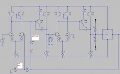
My very first attempt at ndfl and a evening of playing with the simulator.
This is also a realistic sim - not the kind BS so often seen around here such as ultra low THD but with 1 degree of phase margin (ie only workable in simulator land).
ULG of the ndfl front end is 1MHz. The CFB OPS is 3.5MHz. ~80 degree phase margin and clean squarewaves with no overshoot.
The THD-20, 50W into 8 ohms (28.28V peak):
Harmonic Frequency Fourier Normalized Phase Normalized
Number [Hz] Component Component [degree] Phase [deg]
1 2.000e+04 2.827e+01 1.000e+00 -2.30° 0.00°
2 4.000e+04 2.303e-05 8.149e-07 94.90° 97.20°
3 6.000e+04 1.950e-05 6.899e-07 -136.53° -134.23°
4 8.000e+04 3.238e-06 1.145e-07 -92.86° -90.56°
5 1.000e+05 8.918e-06 3.155e-07 52.96° 55.26°
6 1.200e+05 1.655e-06 5.856e-08 -107.33° -105.03°
7 1.400e+05 6.442e-06 2.279e-07 50.49° 52.79°
8 1.600e+05 3.130e-06 1.107e-07 -115.97° -113.67°
9 1.800e+05 8.567e-06 3.031e-07 39.75° 42.05°
Total Harmonic Distortion: 0.000119%
Schemo:
Hi Glenn,
Nice work and nice results.
I have a few questions and observations.
First, I hate to sound ignorant, but I have forgotten what CFB stands for and who came up with the term.
Congratulations on mastering NDFL!
One thing I notice in your output stage that is of possible concern is your use of 0.1 ohm emitter resistors. Such a low value choice of emitter resistor often helps reduce crossover distortion, but at the expense of potentially serious thermal stability problems in the output stage.
BTW, how much bias current are you running in the output stage?
What governed your choice of the 6.8-ohm base stopper resistors?
One thing that can be tricky with base stopper resistors is that they result in an effective ohmic emitter resistance at low frequencies that depends on transistor beta and is modulated by beta droop. If the output transistors have RB=4 ohms at low currents and 7-ohm base stoppers and beta=75, then the effective ohmic resistance seen at the emitter is 0.15 ohms, comparable to the external emitter resistor value of 0.1 ohm.
Cheers,
Bob
Re: Re: Re: Re: Re: Re: CFB OPS
Current feedback, like the YAP output stage 🙂.
Bob Cordell said:First, I hate to sound ignorant, but I have forgotten what CFB stands for and who came up with the term.
Current feedback, like the YAP output stage 🙂.

Hi Andy,
Of course, you only were razzing a bit, never mind. 😉
But to those, not familiar with the history of the CFB/GNF OPS I like to prevent confusion about the 'origin' of this particular kind of OPS.
Regards,
Edmond.
Of course, you only were razzing a bit, never mind. 😉
But to those, not familiar with the history of the CFB/GNF OPS I like to prevent confusion about the 'origin' of this particular kind of OPS.
Regards,
Edmond.
Re: Re: Re: Re: Re: Re: Re: Re: CFB OPS
1942 with valves.
syn08 said:
Beyond his original papers, this helped me a lot in understanding NDFL:
http://www.personal.reading.ac.uk/~shsmchlr/pof/pof20.pdf
BTW, since when is CFB "a trick"? 🙂 CFA is at least as old as patent 4,502,020 by Dave Nelson and Ken Saller, filed in 1983 when they were with Comlinear.
1942 with valves.
Re: CFB OPS
Hi Scott,
What do you mean: CFB or NDFL with valves?
Regards,
Edmond.
scott wurcer said:1942 with valves.
Hi Scott,
What do you mean: CFB or NDFL with valves?
Regards,
Edmond.
Re: Re: Re: Re: Re: Re: CFB OPS
Using various resistance in parallel minimize this problem?
OBS: This schematic is whith Mosfet, I have seen more with Bjts...
Hi CordellBob Cordell said:
One thing I notice in your output stage that is of possible concern is your use of 0.1 ohm emitter resistors. Such a low value choice of emitter resistor often helps reduce crossover distortion, but at the expense of potentially serious thermal stability problems in the output stage.
Using various resistance in parallel minimize this problem?
OBS: This schematic is whith Mosfet, I have seen more with Bjts...
Attachments
Re: Re: Re: Re: Re: Re: CFB OPS
NO!. There are no overload recovery issues with a miller cap connected as feedback around a VAS. As far as that stage goes, all you need is a voltage clamp on the VAS collector.
I've got a few ideas for replacing that funky Rush current amplifier stage.
I agree, but this is just a simulation to test out NDFL combined with CFB. 6.8 ohms seemed like a nice value and the output transistor bias current was set for the lowest distortion (about 200mA).
Cheers,
Glen
Edmond Stuart said:
The overload recovery is complicated by the fact that you have to tame overcharging of two caps: one in the NDFL section and the other in the VAS (Miller cap). This is a well known and notorious problem with NDFL topologies. I see only one solution to this problem: a circuit that limits the charge buildup in both caps at exactly the same time and in a controlled manner, hence the nested Baker clamp. Anyhow, go ahead, but be warned, it's not that easy. We have sweated blood and tears to get it finally right.
NO!. There are no overload recovery issues with a miller cap connected as feedback around a VAS. As far as that stage goes, all you need is a voltage clamp on the VAS collector.
I've got a few ideas for replacing that funky Rush current amplifier stage.
Bob Cordell said:
Hi Glenn,
Nice work and nice results.
I have a few questions and observations.
First, I hate to sound ignorant, but I have forgotten what CFB stands for and who came up with the term.
Congratulations on mastering NDFL!
One thing I notice in your output stage that is of possible concern is your use of 0.1 ohm emitter resistors. Such a low value choice of emitter resistor often helps reduce crossover distortion, but at the expense of potentially serious thermal stability problems in the output stage.
BTW, how much bias current are you running in the output stage?
What governed your choice of the 6.8-ohm base stopper resistors?
One thing that can be tricky with base stopper resistors is that they result in an effective ohmic emitter resistance at low frequencies that depends on transistor beta and is modulated by beta droop. If the output transistors have RB=4 ohms at low currents and 7-ohm base stoppers and beta=75, then the effective ohmic resistance seen at the emitter is 0.15 ohms, comparable to the external emitter resistor value of 0.1 ohm.
Cheers,
Bob
I agree, but this is just a simulation to test out NDFL combined with CFB. 6.8 ohms seemed like a nice value and the output transistor bias current was set for the lowest distortion (about 200mA).
Cheers,
Glen
Re: Re: Re: Re: Re: Re: Re: Re: Re: CFB OPS
That's when Edmond worked it out, evidently (*ducking to avoid airborn false teeth*).
scott wurcer said:
1942 with valves.
That's when Edmond worked it out, evidently (*ducking to avoid airborn false teeth*).
Re: Re: CFB OPS
The fundamental principle of current feedback, the observation that closed loop frequency response drops less rapidly with closed loop gain than with classic feedback, was explicitly made. Walt Jung found it. OTOH I have zero interest in reviving Mikeks debates on the subject.
This is a real brain refresh after Krill and Blowtorch, unfortunately I can't share my latest stuff it really fits here but it is IP.
Edmond Stuart said:
Hi Scott,
What do you mean: CFB or NDFL with valves?
Regards,
Edmond.
The fundamental principle of current feedback, the observation that closed loop frequency response drops less rapidly with closed loop gain than with classic feedback, was explicitly made. Walt Jung found it. OTOH I have zero interest in reviving Mikeks debates on the subject.
This is a real brain refresh after Krill and Blowtorch, unfortunately I can't share my latest stuff it really fits here but it is IP.
Re: Re: Re: CFB OPS
No kidding! Scott, sorry to hear you can't share the latest info. Will it appear in an app note or data sheet eventually?
Glen, please continue when you get the time.
scott wurcer said:This is a real brain refresh after Krill and Blowtorch...
No kidding! Scott, sorry to hear you can't share the latest info. Will it appear in an app note or data sheet eventually?
Glen, please continue when you get the time.
Re: Re: Re: Re: CFB OPS
Eventually, It's a new CFB output stage. People will kick themselve's for not seeing it.
andy_c said:
No kidding! Scott, sorry to hear you can't share the latest info. Will it appear in an app note or data sheet eventually?
Glen, please continue when you get the time.
Eventually, It's a new CFB output stage. People will kick themselve's for not seeing it.
- Home
- Amplifiers
- Solid State
- Bob Cordell Interview: Negative Feedback