Re: Re: distortion
Does the distortion picture change if you remove the load or change the load resistance?
Cheers
Alex
janneman said:Any ideas anyone?
Does the distortion picture change if you remove the load or change the load resistance?
Cheers
Alex
Re: Re: Re: distortion
Good question! The distortion completely disappears when the load is disconnected. But then, it always does, doesn't it? 😉
Jan Didden
x-pro said:
Does the distortion picture change if you remove the load or change the load resistance?
Cheers
Alex
Good question! The distortion completely disappears when the load is disconnected. But then, it always does, doesn't it? 😉
Jan Didden
Re: Re: distortion
Hi Jan,
Normally, crossover distortion produces spikes of alternating polarity, but still there are relative steep glitches near zero crossing (although of the same polarity). So there must be some kind of x-over issue here.
Then we have the asymmetry of the residual. This also may be a result of different gain (beta) of the N and P devices in the output stage, or may be caused by an unexpected beta-droop in one of the O/P trannies.
BTW1, I also looked up in D. Self's "Diagnosing distortion", but failed to positively identify the kind of distortion that you encountered.
BTW2, Fig3, same chapter, shows the x-over spikes of an optimally biased OPS and (opposed to fig.4)....they have the same polarity.
Perhaps, you can figure out what's really going on by playing with a simulator, that is, if you have the right models of course.
Cheers,
Edmond.
edit: while typing this, I missed your last post.
Now it becomes clear that the problem has something to do with current.
janneman said:OK, it's a class-AB output stage. I verified the following:
Bias current: almost no chgange until I really underbias the stage, and then I see the characteristic xover waveform with relatively narrow spikes of alternating polarity.
Feedback take-off: this is on the far lead of the feedback resistor. I always do that to check the actual distortion without possible interference of wrong pick-off point, return currents etc. So that's not it.
It has a star ground for the power traces (supply, load return, local caps) and a separate star ground for the signal returns. These are interconnected with a small resistor. Changing that resistor (between 10 ohms and a short) doesn't make any difference.
The THD shown is around 0.016% at 5kHz, 10VRMS into 8 ohms resistive.
Reading Doug Self's work on 'diagnosing distortion' I tend to think it is some form of supply wiring induction. However, wiggling the supply wiring routing makes almost no change.
............
Any ideas anyone?
Hi Jan,
Normally, crossover distortion produces spikes of alternating polarity, but still there are relative steep glitches near zero crossing (although of the same polarity). So there must be some kind of x-over issue here.
Then we have the asymmetry of the residual. This also may be a result of different gain (beta) of the N and P devices in the output stage, or may be caused by an unexpected beta-droop in one of the O/P trannies.
BTW1, I also looked up in D. Self's "Diagnosing distortion", but failed to positively identify the kind of distortion that you encountered.
BTW2, Fig3, same chapter, shows the x-over spikes of an optimally biased OPS and (opposed to fig.4)....they have the same polarity.
Perhaps, you can figure out what's really going on by playing with a simulator, that is, if you have the right models of course.
Cheers,
Edmond.
edit: while typing this, I missed your last post.
Now it becomes clear that the problem has something to do with current.
Re: Re: Re: Re: distortion
It always does? NO! Think of nonlinear Cob, Cgs, Early effect etc.
Cheers,
Edmond.
janneman said:Good question! The distortion completely disappears when the load is disconnected. But then, it always does, doesn't it? 😉
Jan Didden
It always does? NO! Think of nonlinear Cob, Cgs, Early effect etc.
Cheers,
Edmond.
Re: Re: Re: Re: distortion
In this case have a look at the supply decoupling and layout. The distortion trace looks a bit like a partial coupling of the supplies into the signal path. Try to double the supply decoupling cap on the VAS for one of the rails only at a time and see if that changes the picture.
Cheers
Alex
janneman said:
Good question! The distortion completely disappears when the load is disconnected. But then, it always does, doesn't it? 😉
Jan Didden
In this case have a look at the supply decoupling and layout. The distortion trace looks a bit like a partial coupling of the supplies into the signal path. Try to double the supply decoupling cap on the VAS for one of the rails only at a time and see if that changes the picture.
Cheers
Alex
Hi Jan,
After all these good suggestions, you may also want to look directly on your voltage supply line(s) with the scope - and at various points on those lines (tracks?), triggering with the input signal.
After all these good suggestions, you may also want to look directly on your voltage supply line(s) with the scope - and at various points on those lines (tracks?), triggering with the input signal.
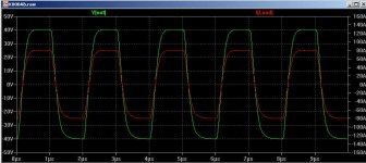
snoopy said:What about supply rejection ?? How does that look ??
What output stage do you plan to couple this with ??
Sorry, I wrongly wrote K200AB in my first post. It is actually the K800AB.
PSR looks fine, especially with seperate regulated rails for the low power circuits.
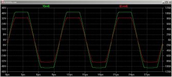
The pic attached should give some idea of the output stage.
Attachments


Macho
Hi Glen,
You really like macho stuff, don't you? Big engines, big amps, ménage à trois.
Nevertheless, the waveforms look very clean. Good luck with this project.
Cheers,
Edmond.
Hi Glen,
You really like macho stuff, don't you? Big engines, big amps, ménage à trois.
Nevertheless, the waveforms look very clean. Good luck with this project.
Cheers,
Edmond.
Re: Macho
I have to complement my manhood somehow.
😀 😀
Edmond Stuart said:Hi Glen,
You really like macho stuff, don't you? Big engines, big amps, ménage à trois.
Nevertheless, the waveforms look very clean. Good luck with this project.
Cheers,
Edmond.
I have to complement my manhood somehow.
😀 😀
Re: Miller compensated dual differential to the extreme
Here is what the final schematic looks like.
For a 2MHz unity loop gain frequency the miller caps are 16pF. Double for 1MHz. Slew rate is 600V/us and 300V/us respectively.
G.Kleinschmidt said:Attached below is a simplified schematic of the finalized front-end design I have developed for a series of my power amps. The first amp to use it will be the K200AB (specs listed on my website).
The design uses a BJT dual LTP input of the current-on-demand H brigde topology buffered and biased by a JFET input buffer.
Each leg of the each LTP runs a quiescent current of 3mA and the VAS runs and quiescent current of 10mA.
Current mirror loads for the LTP's double up the slewrate. Prefectly stable VAS biasing is provided using my VAS biasing scheme in which a bipolar current source biases each VAS transistor via a 1k load resistor presented to each current mirror.
For this sim the closed loop gain was set to 40 (32dB).
The openloop gain was compensated for a unity loop gain crossover frequency of exactly 2MHz.
THD-1kHz at 40V peak output:
0.000011%
THD-20kHz at 40V peak output:
0.000064%
Here is what the final schematic looks like.
For a 2MHz unity loop gain frequency the miller caps are 16pF. Double for 1MHz. Slew rate is 600V/us and 300V/us respectively.
An externally hosted image should be here but it was not working when we last tested it.
OK, OK I'll admit it
you made me look - my screen res is set to 1920x1200 - and I still have to scroll...
you made me look - my screen res is set to 1920x1200 - and I still have to scroll...
Well now, that is really something, Herr Kleinschmidt!
(I don't often contribute here, but follow this thread with interest.)
Regards
(I don't often contribute here, but follow this thread with interest.)
Regards
Hi Glen
There is too many transistors in that circuit.😀
Where is the cascode differential VAS? Or would that be too many transistors even for you? 😀
I’m just kidding.
I see you using THAT arrays. They're nice, but you certainly "pay" for them.... A couple of points I've noticed with these is although they are matched very closely with Ft and noise measuring quite good, I measure Hfe at around 90. This generally isn't a problem but you could buffer the base currents in the mirrors to ensure more equal reflection. You can get away with using little or no degeneration with these. 100R or 47R is overkill. "That" is a reason they cost so much.🙂 Perhaps they’re already degenerated? Not certain but it might explain the lower Hfe figure. Anyway, you only have to connect pin 4 or 11 since they both connect to the substrate.

There is too many transistors in that circuit.😀
Where is the cascode differential VAS? Or would that be too many transistors even for you? 😀
I’m just kidding.
I see you using THAT arrays. They're nice, but you certainly "pay" for them....
A couple of points I've noticed with these is although they are matched very closely with Ft and noise measuring quite good, I measure Hfe at around 90. This generally isn't a problem but you could buffer the base currents in the mirrors to ensure more equal reflection. You can get away with using little or no degeneration with these. 100R or 47R is overkill. "That" is a reason they cost so much.🙂 Perhaps they’re already degenerated? Not certain but it might explain the lower Hfe figure. Anyway, you only have to connect pin 4 or 11 since they both connect to the substrate. Hi Glen and CBS,
I don't think that in most audio amps, you will need very precise current mirrors. It's more important that they don't add to distortion, noise and phase shift.
Cheers,
Edmond.
I don't think that in most audio amps, you will need very precise current mirrors. It's more important that they don't add to distortion, noise and phase shift.
Cheers,
Edmond.
Johan Potgieter said:Well now, that is really something, Herr Kleinschmidt!
(I don't often contribute here, but follow this thread with interest.)
Regards
You're welcome 😉
CBS240 said:Hi Glen
There is too many transistors in that circuit.😀
Where is the cascode differential VAS? Or would that be too many transistors even for you? 😀
I’m just kidding.
I see you using THAT arrays. They're nice, but you certainly "pay" for them....
Hmmm.... The double current mirror circuit I've used with the quad arrays compensates for the base currents. You're quite correct about the emitter degeneration though. I'll drop them down to 20 ohms.
The great thing about these arrays is the fact that they don't have PN junctions between the collectors and the substrate and have minescule device-device capacitances - unlike the MAT and SSM dual matched pairs. They're also cheaper and you get 4 parts instead of 2.
Cheers,
Glen
Re: Amps
Sort of 😉 Inspiration comes from their "Diamond Differential" circuit. There a are lots of other modifications - but the two major topological differences - I only use the dual jfet as a CFP input buffer (with the dual PNP), not as a LTP amplifying stage. The circuit has massive open loop gain and low bandwidth already, so all the jfet stage in the Sansui design contributes is increased distortion with additional gain that just needs to be rolled off.
Also, I use current mirrors on each BJT LTP to double the drive to each VAS stage and increase the slew rate x2. A bipolar current source in included to bias the VAS stages in this arrangement. This also gives significantly lower distortion.
Cheers,
Glen
PHEONIX said:Hello Glen
Are you much of a fan of Sansui power amps.
Regards
Arthur
Sort of 😉 Inspiration comes from their "Diamond Differential" circuit. There a are lots of other modifications - but the two major topological differences - I only use the dual jfet as a CFP input buffer (with the dual PNP), not as a LTP amplifying stage. The circuit has massive open loop gain and low bandwidth already, so all the jfet stage in the Sansui design contributes is increased distortion with additional gain that just needs to be rolled off.
Also, I use current mirrors on each BJT LTP to double the drive to each VAS stage and increase the slew rate x2. A bipolar current source in included to bias the VAS stages in this arrangement. This also gives significantly lower distortion.
Cheers,
Glen
- Home
- Amplifiers
- Solid State
- Bob Cordell Interview: Negative Feedback