PMA said:
Hi Bob,
I had the amp in my workshop for no more than 2 hours, so the number of records collected would be limited.
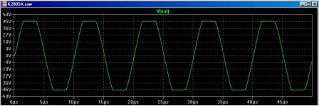
The amp gave 180W into 4 ohms. The output voltage swing with 4 ohms load quite same as without load.
I monitored the whole range of output amplitudes, starting at some 1V. At about 18Vp, the step response shape, that
was RC-like for voltages less or equal 18Vp, started to be slew-rate limited and started to exhibit the behaviour described earlier.
Yes, the observations were similar for no load.
SR measured was 28V/us. The amp was almost unstable to 3.3uF, but handled 390nF with damped oscillations.
I do not know THD 20, I am enclosing THD 1, which was almost same for all power levels and almost copied distortion of my workshop audio generator.
There was an input filter 1k + 100pF (100ns tau), which was insufficient for this amp.
I don’t think that this phenomenon you are describing should be caused by slew rate limiting and the proper implementation of frequency compensation in an amplifier using high levels of GNFB.
I was curious as you your idea so I did a double simulation (pic attached below) my little 10W K10A amp driven with a 1nS rise/fall time squarewave and no input bandwidth filter so as to force it into slewrate limiting (~20V/us).
The amplifier on the left is driven with a 1V squarewave while the one on the right is driver by a 0.1V squarewave. The output of this amp is amplified by 10 and plotted against the output of the other (red/green traces). The step responses between the two are indistinguishable.
Cheers,
Glen
Attachments
Re: Re: variable take off point
I've tried it recently, and I can confirm it works fine... somehow.
You can adjust the little pot and bring the 2nd H down, and this also brings a warm feeling... until you realize the minimum depends on:
a) Signal level. Set a 2nd H minimum at max output power and measure 2nd H up 10dB at 1W output. Or the other way around.
b) Temperature. You need to set up the pot at nominal temperature. Until the amp reaches the thermal equilibrium, you have to live with the 2nd H much higher than without any pot. Of course, if you don't use the amp at nominal power (so the equilibrium temperature is different) then the adjustment impact is, one to another, negative.
c) Frequency. Set it at 20KHz and note the THD10 going up. Or the other way around.
Unfortunately, it seems impossible to find a setting that would, overall, improve the THD performance at all output levels, all frequencies and all temperatures. I was hoping to be able to adjust the 2nd H at a "nominal" functional regime, and otherwise live with the default performance. However, optimizing for a certain regime compromises the overall performance (at other levels, temperatures and frequencies) by a factor of 2...4. Otherwise said, you fix it here and it brokes there.
One to another, you'd better only live with the standard anti-magnetic field measures (short powe wiiring, etc...) as per Self's chapter 14.
I'm expecting a strong dependency of the "little pot effect" on the OPS implementation details, and this won't help in recommending the little pot as a general solution to trim down the 2nd H. If you want, I can send you the details on this "botch job". It's not yet ready for going public.
G.Kleinschmidt said:
Have you ever tried this is a real amp? If so, how sucessfull was it?
I've tried it recently, and I can confirm it works fine... somehow.
You can adjust the little pot and bring the 2nd H down, and this also brings a warm feeling... until you realize the minimum depends on:
a) Signal level. Set a 2nd H minimum at max output power and measure 2nd H up 10dB at 1W output. Or the other way around.
b) Temperature. You need to set up the pot at nominal temperature. Until the amp reaches the thermal equilibrium, you have to live with the 2nd H much higher than without any pot. Of course, if you don't use the amp at nominal power (so the equilibrium temperature is different) then the adjustment impact is, one to another, negative.
c) Frequency. Set it at 20KHz and note the THD10 going up. Or the other way around.
Unfortunately, it seems impossible to find a setting that would, overall, improve the THD performance at all output levels, all frequencies and all temperatures. I was hoping to be able to adjust the 2nd H at a "nominal" functional regime, and otherwise live with the default performance. However, optimizing for a certain regime compromises the overall performance (at other levels, temperatures and frequencies) by a factor of 2...4. Otherwise said, you fix it here and it brokes there.
One to another, you'd better only live with the standard anti-magnetic field measures (short powe wiiring, etc...) as per Self's chapter 14.
I'm expecting a strong dependency of the "little pot effect" on the OPS implementation details, and this won't help in recommending the little pot as a general solution to trim down the 2nd H. If you want, I can send you the details on this "botch job". It's not yet ready for going public.
Miller compensated dual differential to the extreme
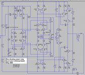
Attached below is a simplified schematic of the finalized front-end design I have developed for a series of my power amps. The first amp to use it will be the K200AB (specs listed on my website).
The design uses a BJT dual LTP input of the current-on-demand H brigde topology buffered and biased by a JFET input buffer.
Each leg of the each LTP runs a quiescent current of 3mA and the VAS runs and quiescent current of 10mA.
Current mirror loads for the LTP's double up the slewrate. Prefectly stable VAS biasing is provided using my VAS biasing scheme in which a bipolar current source biases each VAS transistor via a 1k load resistor presented to each current mirror.
For this sim the closed loop gain was set to 40 (32dB).
The openloop gain was compensated for a unity loop gain crossover frequency of exactly 2MHz.
THD-1kHz at 40V peak output:
0.000011%
THD-20kHz at 40V peak output:
0.000064%
Attachments
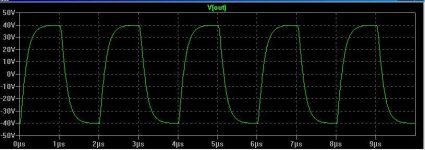
And here is the 1MHz squarewave response swinging 80V peak-peak. This is achived with an squarewave input signal of 2V peak-peak with 1ns rise and fall times and no input signal bandwidth limiting at all. The step response is RC-like with zero overshoot, swinging through 0V at approximately 600V/us.
Attachments

G.Kleinschmidt said:And here is the 1MHz squarewave response swinging 80V peak-peak. This is achived with an squarewave input signal of 2V peak-peak with 1ns rise and fall times and no input signal bandwidth limiting at all. The step response is RC-like with zero overshoot, swinging through 0V at approximately 600V/us.
Nice Job, Glen. Is it measured, or simulated?
Re: Miller compensated dual differential to the extreme
Hi Glen,
Impressive figures, 11 respectively 64ppb.
Not to be picky, but shouldn't you also have a look at the distortion of the front-end including the load of the OPS on the VAS output? In that case you may get different results.
Cheers,
Edmond.
G.Kleinschmidt said:[snip]
THD-1kHz at 40V peak output:
0.000011%
THD-20kHz at 40V peak output:
0.000064%
Hi Glen,
Impressive figures, 11 respectively 64ppb.
Not to be picky, but shouldn't you also have a look at the distortion of the front-end including the load of the OPS on the VAS output? In that case you may get different results.
Cheers,
Edmond.
gain/phase response
Hi Glen,
That looks okay, but not to be picky again, also have look at gain/phase response at the NFB network (by breaking the loop at the 3k9 resistor and grounding the non-input). Eventually, it is only this response that matters with regard to stability.
As the front-end is not 100% symmetrical (because of the i-mirrors), there might be a small difference. Just a matter of check and double check.
Cheers,
Edmond.
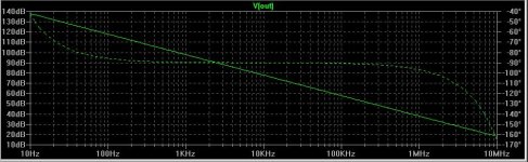
G.Kleinschmidt said:Here is the compensated open loop frequency response, showing the unity loop gain (32dB) crossover at 2MHz.
Hi Glen,
That looks okay, but not to be picky again, also have look at gain/phase response at the NFB network (by breaking the loop at the 3k9 resistor and grounding the non-input). Eventually, it is only this response that matters with regard to stability.
As the front-end is not 100% symmetrical (because of the i-mirrors), there might be a small difference. Just a matter of check and double check.
Cheers,
Edmond.

Re: gain/phase response
THD in sim only, slewrate both. Slew rate is governed by the current that can be delivered to the VAS miller and load capacitance. With a complementary emitter follower pair of fast / low Cob / low Cin CRT driver BJT's to buffer the VAS, >500V/us with a 2MHz unity loop gain is easy.
This is only a simplified front-end sim but it demonstrates that the distortion for this part of the circuit is nothing to worry about.
As a quick test, with a massive 100pF cap loading the VAS output to ground, THD-20 increases from 0.000064% to 0.000069%
BTW, I wasn't expecting any significant differences in the phase/frequency response measured either way, but just to make you happy attached below is a simulation of the actual loop gain only. 😀
I did this by grounding the + input and putting the AC voltage source in series with Rf (the 3.9k resistor) at the output end.
I then plot V(out)/(Vin) where V(in) is the end of the AC voltage source connected to Rf.
As you can see, unity loop gain is definately at 2MHz.
Cheers,
Glen
PMA said:
Nice Job, Glen. Is it measured, or simulated?
THD in sim only, slewrate both. Slew rate is governed by the current that can be delivered to the VAS miller and load capacitance. With a complementary emitter follower pair of fast / low Cob / low Cin CRT driver BJT's to buffer the VAS, >500V/us with a 2MHz unity loop gain is easy.
Edmond Stuart said:
Hi Glen,
Impressive figures, 11 respectively 64ppb.
Not to be picky, but shouldn't you also have a look at the distortion of the front-end including the load of the OPS on the VAS output? In that case you may get different results.
Cheers,
Edmond.
Edmond Stuart said:
Hi Glen,
That looks okay, but not to be picky again, also have look at gain/phase response at the NFB network (by breaking the loop at the 3k9 resistor and grounding the non-input). Eventually, it is only this response that matters with regard to stability.
As the front-end is not 100% symmetrical (because of the i-mirrors), there might be a small difference. Just a matter of check and double check.
Cheers,
Edmond.
This is only a simplified front-end sim but it demonstrates that the distortion for this part of the circuit is nothing to worry about.
As a quick test, with a massive 100pF cap loading the VAS output to ground, THD-20 increases from 0.000064% to 0.000069%
BTW, I wasn't expecting any significant differences in the phase/frequency response measured either way, but just to make you happy attached below is a simulation of the actual loop gain only. 😀
I did this by grounding the + input and putting the AC voltage source in series with Rf (the 3.9k resistor) at the output end.
I then plot V(out)/(Vin) where V(in) is the end of the AC voltage source connected to Rf.
As you can see, unity loop gain is definately at 2MHz.
Cheers,
Glen
Attachments
Re: Re: gain/phase response
OK, I was just wondering.
Now I'm happy 🙂
Cheers,
Edmond.
G.Kleinschmidt said:[snip]
This is only a simplified front-end sim but it demonstrates that the distortion for this part of the circuit is nothing to worry about.
As a quick test, with a massive 100pF cap loading the VAS output to ground, THD-20 increases from 0.000064% to 0.000069%
OK, I was just wondering.
BTW, I wasn't expecting any significant differences in the phase/frequency response measured either way, but just to make you happy attached below is a simulation of the actual loop gain only. 😀
I did this by grounding the + input and putting the AC voltage source in series with Rf (the 3.9k resistor) at the output end.
I then plot V(out)/(Vin) where V(in) is the end of the AC voltage source connected to Rf.
As you can see, unity loop gain is definately at 2MHz.
Cheers,
Glen
Now I'm happy 🙂
Cheers,
Edmond.
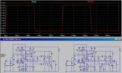
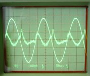
janneman said:If I may make a small excursion into actual hardware 😉 , if you see this on your scope, what mechanism would you think would cause this particular type of distortion?
Jan Didden
Hi Jan,
At first glance I'd say it's crossover distortion of a ordinary class-B OPS, although normally, one should expect a slightly different picture from such OPS.
Another possibility is an incorrect NFB take-off point inside the OPS, or even, it's a combination of both.
Cheers,
Edmond.
janneman said:If I may make a small excursion into actual hardware 😉 , if you see this on your scope, what mechanism would you think would cause this particular type of distortion?
Jan Didden
Crossover distortion are typically 3rd harmonic. The picture showing the signal after removing the fundamental is mostly 2nd harmonic which suggest either a magnetic effect (usually a coupling between the power bars into the FB loop) and/or an asymmetry in the layout of the FB loop.
What about supply rejection ?? How does that look ??
What output stage do you plan to couple this with ??
What output stage do you plan to couple this with ??
distortion
Hi Jan,
Can you give us a little more information. Is the distortion from a MOSFET or BJT output stage? (I guess BJT) Also, what's the class, B, AB, AAB? And what were the test conditions (power, load, Iq etc.).
Anyhow, it's clear that more than one mechanism is involved that creates such kind of distortion.
Cheers,
Edmond.
Some more super dual diff front end sims
This this I have increased the supply rail voltages to +/-60V for a bit of extra head room. I have also doubled the value of the miller compensation capacitors to bring the unity loop gain frequency to 1MHz and added a clipping voltage clamp to the VAS collectors to prevent the VAS cascode transistors from saturating.
Due to the 1k LTP current mirror load resistors used for VAS biasing, the drive to each VAS transistors in this design is automatically limited during clipping.
With the currently proportioned VAS emitter degeneration and LTP "tail" current and VAS biasing voltage, the max VAS transistor current is 3*Iq.
This means that noting besides a voltage clamp at the VAS collectors is required to control clipping performance.
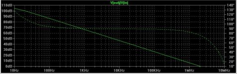
Attached below is a sim of the amplifier clipping, overdriven with a 100kHz sinewave. The VAS collector voltage clamp is set to +/-45V.
This this I have increased the supply rail voltages to +/-60V for a bit of extra head room. I have also doubled the value of the miller compensation capacitors to bring the unity loop gain frequency to 1MHz and added a clipping voltage clamp to the VAS collectors to prevent the VAS cascode transistors from saturating.
Due to the 1k LTP current mirror load resistors used for VAS biasing, the drive to each VAS transistors in this design is automatically limited during clipping.
With the currently proportioned VAS emitter degeneration and LTP "tail" current and VAS biasing voltage, the max VAS transistor current is 3*Iq.
This means that noting besides a voltage clamp at the VAS collectors is required to control clipping performance.
Attached below is a sim of the amplifier clipping, overdriven with a 100kHz sinewave. The VAS collector voltage clamp is set to +/-45V.
Attachments
As expected the slewrate has halved along with the unity loop gain frequency.
Attached below is the 500kHz squarewave response at 80Vp-p output.
The distortion has also risen a little at HF.
THD-1kHz 40V peak:
0.000007%
THD-20kHz 40V peak:
0.000088%
THD-100kHz 40V peak:
0.000956%
Attached below is the 500kHz squarewave response at 80Vp-p output.
The distortion has also risen a little at HF.
THD-1kHz 40V peak:
0.000007%
THD-20kHz 40V peak:
0.000088%
THD-100kHz 40V peak:
0.000956%
Attachments
Re: distortion
OK, it's a class-AB output stage. I verified the following:
Bias current: almost no chgange until I really underbias the stage, and then I see the characteristic xover waveform with relatively narrow spikes of alternating polarity.
Feedback take-off: this is on the far lead of the feedback resistor. I always do that to check the actual distortion without possible interference of wrong pick-off point, return currents etc. So that's not it.
It has a star ground for the power traces (supply, load return, local caps) and a separate star ground for the signal returns. These are interconnected with a small resistor. Changing that resistor (between 10 ohms and a short) doesn't make any difference.
The THD shown is around 0.016% at 5kHz, 10VRMS into 8 ohms resistive.
Reading Doug Self's work on 'diagnosing distortion' I tend to think it is some form of supply wiring induction. However, wiggling the supply wiring routing makes almost no change.
Attached again the waveform for completeness. The very low-level hash that can be seen is due to the PC monitor, and disappears when I shut that off.
Any ideas anyone?
Edmond Stuart said:Hi Jan,
Can you give us a little more information. Is the distortion from a MOSFET or BJT output stage? (I guess BJT) Also, what's the class, B, AB, AAB? And what were the test conditions (power, load, Iq etc.).
Anyhow, it's clear that more than one mechanism is involved that creates such kind of distortion.
Cheers,
Edmond.
OK, it's a class-AB output stage. I verified the following:
Bias current: almost no chgange until I really underbias the stage, and then I see the characteristic xover waveform with relatively narrow spikes of alternating polarity.
Feedback take-off: this is on the far lead of the feedback resistor. I always do that to check the actual distortion without possible interference of wrong pick-off point, return currents etc. So that's not it.
It has a star ground for the power traces (supply, load return, local caps) and a separate star ground for the signal returns. These are interconnected with a small resistor. Changing that resistor (between 10 ohms and a short) doesn't make any difference.
The THD shown is around 0.016% at 5kHz, 10VRMS into 8 ohms resistive.
Reading Doug Self's work on 'diagnosing distortion' I tend to think it is some form of supply wiring induction. However, wiggling the supply wiring routing makes almost no change.
Attached again the waveform for completeness. The very low-level hash that can be seen is due to the PC monitor, and disappears when I shut that off.
Any ideas anyone?
Attachments
Re: Re: distortion
Wiggling the power lines does not necessary help. Twist the +/- supply lines and see if it does any good. Remeber, magnetics go through loops not through wires. Keeping the supply lines perpendicular to any signal lines (in particular the feedback return) may also help.
For diagnosis purposes only (otherwise it's of little use in practice, for the reasons I've posted before) it might be useful to install Edmond's little pot. This will help in nulling down any 2nd order distortions due to asymmetries in the layout, at a certain frequency and output level.
janneman said:
OK, it's a class-AB output stage. I verified the following:
Bias current: almost no chgange until I really underbias the stage, and then I see the characteristic xover waveform with relatively narrow spikes of alternating polarity.
Feedback take-off: this is on the far lead of the feedback resistor. I always do that to check the actual distortion without possible interference of wrong pick-off point, return currents etc. So that's not it.
It has a star ground for the power traces (supply, load return, local caps) and a separate star ground for the signal returns. These are interconnected with a small resistor. Changing that resistor (between 10 ohms and a short) doesn't make any difference.
The THD shown is around 0.016% at 5kHz, 10VRMS into 8 ohms resistive.
Reading Doug Self's work on 'diagnosing distortion' I tend to think it is some form of supply wiring induction. However, wiggling the supply wiring routing makes almost no change.
Attached again the waveform for completeness. The very low-level hash that can be seen is due to the PC monitor, and disappears when I shut that off.
Any ideas anyone?
Wiggling the power lines does not necessary help. Twist the +/- supply lines and see if it does any good. Remeber, magnetics go through loops not through wires. Keeping the supply lines perpendicular to any signal lines (in particular the feedback return) may also help.
For diagnosis purposes only (otherwise it's of little use in practice, for the reasons I've posted before) it might be useful to install Edmond's little pot. This will help in nulling down any 2nd order distortions due to asymmetries in the layout, at a certain frequency and output level.
- Home
- Amplifiers
- Solid State
- Bob Cordell Interview: Negative Feedback