PMA said:Polystyrene.
What brand polystyrene? Do they go down below 30 pF?
What do you think about the WIMA FKP-2 polypropylene film and foil caps?
Thanks!
Bob
I have an old stock, TESLA nad TGL production. They start at 10pF.
WIMA FKP-2 starts at 33pF. These are fine capacitors, IMHO.
WIMA FKP-2 starts at 33pF. These are fine capacitors, IMHO.
I have about two pounds of assorted small value polystyrenes bargained from a thrift store -- sort of a lifetime supply.
For experimentation I often use small adjustable air cores, mostly salvaged from receivers and the like.
- Klaus
For experimentation I often use small adjustable air cores, mostly salvaged from receivers and the like.
- Klaus
Re: Choice of small-value capacitors
I'm still using SM's but I only need to make one or two.
Bob Cordell said:Virtually all amplifiers using negative feedback employ one or more small-value capacitors in the compensation network, and often elsewhere as well. We're talking capacitances that often are in the range of 5pF to 100 pF.
We all know that it is important to pick good-quality passive components. The quality of the capacitor chosen for use in Miller compensation, for example, can be quite influential.
I'm interested to know what types of capacitors people are using in these small-value locations in power amplifiers and what their experience has been.
Thanks,
Bob
I'm still using SM's but I only need to make one or two.
PMA said:I have an old stock, TESLA nad TGL production. They start at 10pF.
WIMA FKP-2 starts at 33pF. These are fine capacitors, IMHO.
Agreed, I wish they made them smaller, I'm not that comfortable with
using them in series to get smaller values.
T
Re: Re: Choice of small-value capacitors
lineup said:
🙂
Until now, I have used ceramics.
Simply because of I can easily find and buy such in my country.
Ceramics NP0 quality are also cheap.
For my next amplifier project, seems I would have to rethink!
Ever since reading the article on capacitors by Jung and Marsh I have been wary of using ceramics of any kind. However, I do sometimes wonder what experince people have had with COG ceramics, as they apparently do not have the ferro-electric properties of X7R et al.
Any opinions on COG ceramics?
Thanks,
Bob
Bob,
In the white paper for the Jensen/Hardy 990 discrete Opamp this is discussed. Bottom line, don't be afraid of COG ceramics for audio.
- Klaus
In the white paper for the Jensen/Hardy 990 discrete Opamp this is discussed. Bottom line, don't be afraid of COG ceramics for audio.
- Klaus
Re: Re: Re: Choice of small-value capacitors
Bob Cordell said:lineup said:Ever since reading the article on capacitors by Jung and Marsh I have been wary of using ceramics of any kind. However, I do sometimes wonder what experince people have had with COG ceramics, as they apparently do not have the ferro-electric properties of X7R et al.
Any opinions on COG ceramics?
Hi Bob,
Not sure if you've seen these yet, but Cyril Bateman has put his capacitor distortion articles from Electronics world up on his web site here. His measurements show the C0G ceramics to be quite good.
BTW, his site has limited bandwidth. If the bandwidth requirements are exceeded before you've downloaded all of them, it comes back automatically in an hour or so.
Re: Re: Re: Choice of small-value capacitors
Bob Cordell said:lineup said:
🙂
Until now, I have used ceramics.
Simply because of I can easily find and buy such in my country.
Ceramics NP0 quality are also cheap.
For my next amplifier project, seems I would have to rethink!
Ever since reading the article on capacitors by Jung and Marsh I have been wary of using ceramics of any kind. However, I do sometimes wonder what experince people have had with COG ceramics, as they apparently do not have the ferro-electric properties of X7R et al.
Any opinions on COG ceramics?
Thanks,
Bob
Why I have used ceramics?
Really not always.
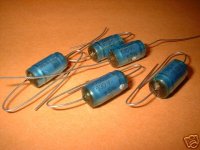
I have a package of polypropylene AXIAL small:
ERO KP1838, 2.5%, 630V -
They range from 100pF, 220pF to 4700pF.
I bought it on SALE, from a surplus .... some do not know what they sell out!!!
See attachment picture.
But, although two 100pF in series make one 50 pF,
I still use ceramics NP0 for lower values.
Like for example 22pF for compensate NE5534, for gains below x5.
If using ceramics, I think NP0 is the best I can get.Ceramic capacitors differ in terms of electrostatic material, the insulation between the plates of a multilayer capacitor.
Ceramic COG (NPO) capacitors have a high Q, low K, temperature-compensated dielectric and
stable electrical properties under varying voltage, temperature, frequency and time.
They are suitable for low-lost circuits and for timing and tuning applications.
It should be noted,
that the '0' in NP0, stands for ZERO temp koefficient.
That is, capacitance value does not change (hardly any) with temperature. Neither + or -
Of course, if I can get my hands on good plastic film caps
I would go for them, any time.
At least for my HIFI Audio circuits 🙂
Regards
lineup
Attachments
Miller compensation connection
This post addresses a question that Glen raised over in the Error Correction thread. Since the issue is Miller feedback compensation, it is more appropriate to address it here in this thread.
The discussion concerned the question of picking off the Miller compensation feedback capacitor connection from the high-impedance VAS collector as opposed to from the following emitter follower pre-driver. The former is the way it is usually done. In some cases, there are benefits to picking it off after the buffering so that the Miller capacitance or network does not load the high impedance VAS node. One example is where we use T compensation, where the first capacitor usually wants to be larger than the second capacitor and the shunt resistor can impose a significant load on the VAS collector circuit. The “outer” pick-off point can also be advantageous in TMC arrangements as well.
I had asserted that picking off the compensation after the pre-driver emitter follower was just as good as picking it off directly from the high-impedance VAS collector, both from a frequency response point of view and from a distortion point of view. Although the behavior of the two stages is not identical, it is largely the same because the voltage at the pick-off end of the Miller capacitor is essentially the same in both cases, since the pre-driver EF has a gain of essentially unity.
Glen asserted that it is bad to pick off after the pre-driver EF because that takes away the shunt feedback effect of the Miller capacitor on the high-impedance VAS collector node. That desirable action reduces the output impedance of the VAS collector node, making it less vulnerable to the nonlinear capacitance effects of the collector-base capacitance of the pre-driver transistor. He asserts that distortion will increase when the capacitor is connected on the “outside” to the emitter of the pre-driver EF because the VAS collector node is left in a high-impedance state. It is easy to see how this would seem to be intuitively correct, but it is not. This is why it is sometimes very important to do sanity checks on our intuition.
Glen also seemed to imply that the outer connection of the Miller capacitor foregoes the effects of pole-splitting that we enjoy with the conventional “inner” miller compensation connection. In fact, simulation shows that the frequency response of the combined VAS and pre-driver stage is essentially the same for both connections.
Forgive me, Glen, if I have mis-stated your position.
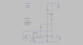
The simulation was done with two transistors, a 2N5550 acting as the VAS and biased at 10 mA with a 22 ohm emitter resistor, and an MJE243 acting as the pre-driver emitter follower, also biased at 10 mA. A 30 pF Miller compensation capacitor was used in both connections. The base of the VAS stage was driven from a 10k signal source. The arrangement was biased from +/- 50V rails and operated at 49 V p-p at 20 kHz. THD-20 distortion percentages were as follows for the inner and outer connections (note that this is essentially distortion of the arrangement absent any global negative feedback):
Distortion Inner Outer
THD-20:_ 0.411_____ 0.411
2_______ 0.412_____ 0.411
3_______ 0.03______ 0.03
4_______ 0.00255___ 0.0027
5_______ 0.00055___ 0.00055
6_______ 0.000069__ 0.000078
7_______ 0.000020__ 0.000020
The behavior of the two different connections is remarkably similar.
Cheers,
Bob
This post addresses a question that Glen raised over in the Error Correction thread. Since the issue is Miller feedback compensation, it is more appropriate to address it here in this thread.
The discussion concerned the question of picking off the Miller compensation feedback capacitor connection from the high-impedance VAS collector as opposed to from the following emitter follower pre-driver. The former is the way it is usually done. In some cases, there are benefits to picking it off after the buffering so that the Miller capacitance or network does not load the high impedance VAS node. One example is where we use T compensation, where the first capacitor usually wants to be larger than the second capacitor and the shunt resistor can impose a significant load on the VAS collector circuit. The “outer” pick-off point can also be advantageous in TMC arrangements as well.
I had asserted that picking off the compensation after the pre-driver emitter follower was just as good as picking it off directly from the high-impedance VAS collector, both from a frequency response point of view and from a distortion point of view. Although the behavior of the two stages is not identical, it is largely the same because the voltage at the pick-off end of the Miller capacitor is essentially the same in both cases, since the pre-driver EF has a gain of essentially unity.
Glen asserted that it is bad to pick off after the pre-driver EF because that takes away the shunt feedback effect of the Miller capacitor on the high-impedance VAS collector node. That desirable action reduces the output impedance of the VAS collector node, making it less vulnerable to the nonlinear capacitance effects of the collector-base capacitance of the pre-driver transistor. He asserts that distortion will increase when the capacitor is connected on the “outside” to the emitter of the pre-driver EF because the VAS collector node is left in a high-impedance state. It is easy to see how this would seem to be intuitively correct, but it is not. This is why it is sometimes very important to do sanity checks on our intuition.
Glen also seemed to imply that the outer connection of the Miller capacitor foregoes the effects of pole-splitting that we enjoy with the conventional “inner” miller compensation connection. In fact, simulation shows that the frequency response of the combined VAS and pre-driver stage is essentially the same for both connections.
Forgive me, Glen, if I have mis-stated your position.
The simulation was done with two transistors, a 2N5550 acting as the VAS and biased at 10 mA with a 22 ohm emitter resistor, and an MJE243 acting as the pre-driver emitter follower, also biased at 10 mA. A 30 pF Miller compensation capacitor was used in both connections. The base of the VAS stage was driven from a 10k signal source. The arrangement was biased from +/- 50V rails and operated at 49 V p-p at 20 kHz. THD-20 distortion percentages were as follows for the inner and outer connections (note that this is essentially distortion of the arrangement absent any global negative feedback):
Distortion Inner Outer
THD-20:_ 0.411_____ 0.411
2_______ 0.412_____ 0.411
3_______ 0.03______ 0.03
4_______ 0.00255___ 0.0027
5_______ 0.00055___ 0.00055
6_______ 0.000069__ 0.000078
7_______ 0.000020__ 0.000020
The behavior of the two different connections is remarkably similar.
Cheers,
Bob
Attachments
Re: Miller compensation connection
You've done a very good job of mis-stating my position in just about every possible aspect.
I did not say that picking off the miller compensation capacitor from the first emitter follower (or driver in a double EF OPS) was a "bad idea", nor did I imply that there were no benefits to be had (eg > slew rate) with the connection.
I said that in the moving the miller comp connection from the VAS collector doesn't always result in lower THD. In a lot of cases it is lower. In some cases there is hardly any difference and in some cases it can be signifcantly higher.
I demonstrated this fact by providing a simulation for everybody to see of a design in which the connection yielded significantly higher THD-20.
I've had similar results from applying TMC to such designs and so had Edmond. Maybe you could ask him for more design examples.
In these examples you can ignore what we have found and assert that "from a distortion point of view" the performance is just as good if you wan't, but it demonstratably is not.
Nope. I asserted that the combined open loop frequency response characteristics of the stages enclosed within the miller loop are much less venerable to the non-linear input capacitance of the first EF with the miller cap connected to the VAS collector. That is a demonstratable fact. The miller capacitance is then effectively the dominant capacitive load on the VAS collector.
I offered this as a further elaboration of the circuit operation further to Edmonds postulation that the significantly higher THD sometimes yielded by the EF miller compensation connection may be have something to do with the cancellation effects of distortion products.
Exactly how much of a role the open loop frequency response variation caused by (VASgm * the non-linear EF load capacitance) plays in the higher THD yielded in some specific design cases by the "outer" miller cap connection, I don't know, and it seems that neither do you.
Cheers,
Glen
Bob Cordell said:The discussion concerned the question of picking off the Miller compensation feedback capacitor connection from the high-impedance VAS collector as opposed to from the following emitter follower pre-driver. The former is the way it is usually done. In some cases, there are benefits to picking it off after the buffering so that the Miller capacitance or network does not load the high impedance VAS node. One example is where we use T compensation, where the first capacitor usually wants to be larger than the second capacitor and the shunt resistor can impose a significant load on the VAS collector circuit. The “outer” pick-off point can also be advantageous in TMC arrangements as well.
I had asserted that picking off the compensation after the pre-driver emitter follower was just as good as picking it off directly from the high-impedance VAS collector, both from a frequency response point of view and from a distortion point of view. Although the behavior of the two stages is not identical, it is largely the same because the voltage at the pick-off end of the Miller capacitor is essentially the same in both cases, since the pre-driver EF has a gain of essentially unity.
Forgive me, Glen, if I have mis-stated your position.
You've done a very good job of mis-stating my position in just about every possible aspect.
I did not say that picking off the miller compensation capacitor from the first emitter follower (or driver in a double EF OPS) was a "bad idea", nor did I imply that there were no benefits to be had (eg > slew rate) with the connection.
I said that in the moving the miller comp connection from the VAS collector doesn't always result in lower THD. In a lot of cases it is lower. In some cases there is hardly any difference and in some cases it can be signifcantly higher.
I demonstrated this fact by providing a simulation for everybody to see of a design in which the connection yielded significantly higher THD-20.
I've had similar results from applying TMC to such designs and so had Edmond. Maybe you could ask him for more design examples.
In these examples you can ignore what we have found and assert that "from a distortion point of view" the performance is just as good if you wan't, but it demonstratably is not.
Bob Cordell said:Glen asserted that it is bad to pick off after the pre-driver EF because that takes away the shunt feedback effect of the Miller capacitor on the high-impedance VAS collector node. That desirable action reduces the output impedance of the VAS collector node, making it less vulnerable to the nonlinear capacitance effects of the collector-base capacitance of the pre-driver transistor. He asserts that distortion will increase when the capacitor is connected on the “outside” to the emitter of the pre-driver EF because the VAS collector node is left in a high-impedance state. It is easy to see how this would seem to be intuitively correct, but it is not. This is why it is sometimes very important to do sanity checks on our intuition.
Glen also seemed to imply that the outer connection of the Miller capacitor foregoes the effects of pole-splitting that we enjoy with the conventional “inner” miller compensation connection. In fact, simulation shows that the frequency response of the combined VAS and pre-driver stage is essentially the same for both connections.[/B]
Nope. I asserted that the combined open loop frequency response characteristics of the stages enclosed within the miller loop are much less venerable to the non-linear input capacitance of the first EF with the miller cap connected to the VAS collector. That is a demonstratable fact. The miller capacitance is then effectively the dominant capacitive load on the VAS collector.
I offered this as a further elaboration of the circuit operation further to Edmonds postulation that the significantly higher THD sometimes yielded by the EF miller compensation connection may be have something to do with the cancellation effects of distortion products.
Exactly how much of a role the open loop frequency response variation caused by (VASgm * the non-linear EF load capacitance) plays in the higher THD yielded in some specific design cases by the "outer" miller cap connection, I don't know, and it seems that neither do you.
Cheers,
Glen
Re: Re: Miller compensation connection
Hi Glen,
I'm digging in my old files, but failed to find the one that shows this "anomaly". Perhaps you can give me a hint. Was it your 12W class-A amp? Also, you might have a look at our e-mails, if you still have them of course. Mine are lost due to a HD crash.
Cheers,
Edmond.
G.Kleinschmidt said:[snip]
I demonstrated this fact by providing a simulation for everybody to see of a design in which the connection yielded significantly higher THD-20.
I've had similar results from applying TMC to such designs and so had Edmond. Maybe you could ask him for more design examples.
[snip]
Cheers,
Glen
Hi Glen,
I'm digging in my old files, but failed to find the one that shows this "anomaly". Perhaps you can give me a hint. Was it your 12W class-A amp? Also, you might have a look at our e-mails, if you still have them of course. Mine are lost due to a HD crash.
Cheers,
Edmond.
Re: Re: Re: Miller compensation connection
Hi Edmond. Sorry to hear about you hard drive crash. I don't recall what the scenario was with the 12W amp anymore, but I recall reporting that the mod was giving me higher THD in some sims using Multisim (confused as to why) and you reported back that you have found the same thing using MCap (also confused as to why).
That was the last I though about it until the issue of the alternate miller cap connection came up in the BJT Vs MOSFET thread. Sorry! 🙁
Also, as an aside, I don't think that simulations of just a VAS stage with an EF enclosed within the miller loop demonstrates much. A complete amplifier design, loop closed with a valid OPS actually loading the VAS is needed here - like that provided in post 2949 here (in which the "anomaly" is demonstratable and repeatable):
http://www.diyaudio.com/forums/showthread.php?postid=1494688#post1494688
Cheers,
Glen
Edmond Stuart said:
Hi Glen,
I'm digging in my old files, but failed to find the one that shows this "anomaly". Perhaps you can give me a hint. Was it your 12W class-A amp? Also, you might have a look at our e-mails, if you still have them of course. Mine are lost due to a HD crash.
Cheers,
Edmond.
Hi Edmond. Sorry to hear about you hard drive crash. I don't recall what the scenario was with the 12W amp anymore, but I recall reporting that the mod was giving me higher THD in some sims using Multisim (confused as to why) and you reported back that you have found the same thing using MCap (also confused as to why).
That was the last I though about it until the issue of the alternate miller cap connection came up in the BJT Vs MOSFET thread. Sorry! 🙁
Also, as an aside, I don't think that simulations of just a VAS stage with an EF enclosed within the miller loop demonstrates much. A complete amplifier design, loop closed with a valid OPS actually loading the VAS is needed here - like that provided in post 2949 here (in which the "anomaly" is demonstratable and repeatable):
http://www.diyaudio.com/forums/showthread.php?postid=1494688#post1494688
Cheers,
Glen
Re: Re: Miller compensation connection
Hi Glen,
I'm sorry if I mis-stated your position. I am therefore a bit puzzled by the fact that you referred to my stated position as "nonsense". That was rude. Nobody likes to have their words characterized as nonsense, especially if the disagreement is subtle or semantical. Your statements and mine in the other thread speak for themselves. I think that your statements showed that you were being misled by your intuition, but I could be wrong. That sometimes happens to me as well. Its nothing to be defensive about.
It sounds like we are in agreement with the following two points:
There is usually no performance or behavioral penalty for using the "outside" connection for the Miller capacitor. Pole-splitting behavior is essentially the same. Open-loop distortion of the pair, with the inside connection or the outside connection is essentially the same.
In many circuits there is no distortion advantage to doing so.
I never implied that I was employing that connection to achieve lower distortion by enclosing the pre-driver EF in the Miller loop, as you know. However, I did say that in some cases it was desirable to not load the VAS collector with the compensation network.
Are you are referring to the "simulation" you showed in your last post on the subject where you accompanied the drawing with a question rather than results? That did not seem to prove anything insofar as the question at hand.
Cheers,
Bob
G.Kleinschmidt said:
You've done a very good job of mis-stating my position in just about every possible aspect.
I did not say that picking off the miller compensation capacitor from the first emitter follower (or driver in a double EF OPS) was a "bad idea", nor did I imply that there were no benefits to be had (eg > slew rate) with the connection.
I said that in the moving the miller comp connection from the VAS collector doesn't always result in lower THD. In a lot of cases it is lower. In some cases there is hardly any difference and in some cases it can be signifcantly higher.
I demonstrated this fact by providing a simulation for everybody to see of a design in which the connection yielded significantly higher THD-20.
I've had similar results from applying TMC to such designs and so had Edmond. Maybe you could ask him for more design examples.
In these examples you can ignore what we have found and assert that "from a distortion point of view" the performance is just as good if you wan't, but it demonstratably is not.
Nope. I asserted that the combined open loop frequency response characteristics of the stages enclosed within the miller loop are much less venerable to the non-linear input capacitance of the first EF with the miller cap connected to the VAS collector. That is a demonstratable fact. The miller capacitance is then effectively the dominant capacitive load on the VAS collector.
I offered this as a further elaboration of the circuit operation further to Edmonds postulation that the significantly higher THD sometimes yielded by the EF miller compensation connection may be have something to do with the cancellation effects of distortion products.
Exactly how much of a role the open loop frequency response variation caused by (VASgm * the non-linear EF load capacitance) plays in the higher THD yielded in some specific design cases by the "outer" miller cap connection, I don't know, and it seems that neither do you.
Cheers,
Glen
Hi Glen,
I'm sorry if I mis-stated your position. I am therefore a bit puzzled by the fact that you referred to my stated position as "nonsense". That was rude. Nobody likes to have their words characterized as nonsense, especially if the disagreement is subtle or semantical. Your statements and mine in the other thread speak for themselves. I think that your statements showed that you were being misled by your intuition, but I could be wrong. That sometimes happens to me as well. Its nothing to be defensive about.
It sounds like we are in agreement with the following two points:
There is usually no performance or behavioral penalty for using the "outside" connection for the Miller capacitor. Pole-splitting behavior is essentially the same. Open-loop distortion of the pair, with the inside connection or the outside connection is essentially the same.
In many circuits there is no distortion advantage to doing so.
I never implied that I was employing that connection to achieve lower distortion by enclosing the pre-driver EF in the Miller loop, as you know. However, I did say that in some cases it was desirable to not load the VAS collector with the compensation network.
Are you are referring to the "simulation" you showed in your last post on the subject where you accompanied the drawing with a question rather than results? That did not seem to prove anything insofar as the question at hand.
Cheers,
Bob
Re: Re: Re: Re: Miller compensation connection

BTW, I'm still digging in order to provide more evidence for this peculiar phenomenon.
Cheers,
Edmond.
G.Kleinschmidt said:[snip]
Also, as an aside, I don't think that simulations of just a VAS stage with an EF enclosed within the miller loop demonstrates much. A complete amplifier design, loop closed with a valid OPS actually loading the VAS is needed here - like that provided in post 2949 here (in which the "anomaly" is demonstratable and repeatable):
http://www.diyaudio.com/forums/showthread.php?postid=1494688#post1494688
Cheers,
Glen
BTW, I'm still digging in order to provide more evidence for this peculiar phenomenon.
Cheers,
Edmond.
Re: Re: Re: Miller compensation connection
There is a degree of irony with that complaint coming from you.
I never said that you did. Why do you keep defending yourself against a non existant accusation?
As clearly stated with the post number and even a direct hyper-link provided (to avoid confusion 🙄 ), in my last post I was referring to the simulation in which the THD-20 is shown to increase ~10% with the "outer" cap connection.
As for your dismissal of the drawing with the accompanying (ignored) question in the other thread, am I supposed to take that as seriously as your claim that you don't actually know which "simulation" I was referring to in my post above?
Am I wasting my time in this discussion for any good reason?
Cheers,
Glen
Bob Cordell said:I'm sorry if I mis-stated your position. I am therefore a bit puzzled by the fact that you referred to my stated position as "nonsense". That was rude. Nobody likes to have their words characterized as nonsense, especially if the disagreement is subtle or semantical.
There is a degree of irony with that complaint coming from you.
Bob Cordell said:I never implied that I was employing that connection to achieve lower distortion by enclosing the pre-driver EF in the Miller loop, as you know. .[/B]
I never said that you did. Why do you keep defending yourself against a non existant accusation?
Bob Cordell said:Are you are referring to the "simulation" you showed in your last post on the subject where you accompanied the drawing with a question rather than results? That did not seem to prove anything insofar as the question at hand.[/B]
As clearly stated with the post number and even a direct hyper-link provided (to avoid confusion 🙄 ), in my last post I was referring to the simulation in which the THD-20 is shown to increase ~10% with the "outer" cap connection.
As for your dismissal of the drawing with the accompanying (ignored) question in the other thread, am I supposed to take that as seriously as your claim that you don't actually know which "simulation" I was referring to in my post above?
Am I wasting my time in this discussion for any good reason?
Cheers,
Glen
Re: Re: Re: Re: Miller compensation connection
10% difference? yes, I'd say our time is being wasted
given the real occurrence of cancellations of individual terms in an overall amp's nonlinearity by very specific and difficult to predict/design for relations between device nonlinearity/bias/gain/feedback distribution(across stages from local degen, Miller to TMC to global) 10% difference in THD isn't significant as a test of how/where to best apply negative feedback
in my opinion negative feedback principles are best illustrated by applying it for order(s) of magnitude distortion reductions
G.Kleinschmidt said:
...As clearly stated with the post number and even a direct hyper-link provided (to avoid confusion 🙄 ), in my last post I was referring to the simulation in which the THD-20 is shown to increase ~10% with the "outer" cap connection.
...Am I wasting my time in this discussion for any good reason?
Cheers,
Glen
10% difference? yes, I'd say our time is being wasted
given the real occurrence of cancellations of individual terms in an overall amp's nonlinearity by very specific and difficult to predict/design for relations between device nonlinearity/bias/gain/feedback distribution(across stages from local degen, Miller to TMC to global) 10% difference in THD isn't significant as a test of how/where to best apply negative feedback
in my opinion negative feedback principles are best illustrated by applying it for order(s) of magnitude distortion reductions
Re: Re: Re: Re: Miller compensation connection
Gently trying to correct you on anything is a complete waste of time. The fact remains that the string of posts clearly shows that your intuition was leading you astray and that a proper simulation showed the correct interpretation. I never tried to rub your nose in it, but you just cannot leave well enough alone. You are a very smart guy and contribute a lot of good stuff, but your contrarian nit-picking is truly tiresome.
Bob
G.Kleinschmidt said:
There is a degree of irony with that complaint coming from you.
I never said that you did. Why do you keep defending yourself against a non existant accusation?
As clearly stated with the post number and even a direct hyper-link provided (to avoid confusion 🙄 ), in my last post I was referring to the simulation in which the THD-20 is shown to increase ~10% with the "outer" cap connection.
As for your dismissal of the drawing with the accompanying (ignored) question in the other thread, am I supposed to take that as seriously as your claim that you don't actually know which "simulation" I was referring to in my post above?
Am I wasting my time in this discussion for any good reason?
Cheers,
Glen
Gently trying to correct you on anything is a complete waste of time. The fact remains that the string of posts clearly shows that your intuition was leading you astray and that a proper simulation showed the correct interpretation. I never tried to rub your nose in it, but you just cannot leave well enough alone. You are a very smart guy and contribute a lot of good stuff, but your contrarian nit-picking is truly tiresome.
Bob
Re: Re: Re: Re: Re: Miller compensation connection
Agreed.
Here's an example on how much "10%" means. I'm working on a new design, not an outstanding or totally new topology, 2SK170/2SJ74 JFET diff pairs input, 2SK1530/2SJ201 output, dual pole compensation, just trying to push some ideas to the limit.
Simulators (PSpice, LTSpice, MicroCap, latest device models including Andy's for the power MOSFETs) are all tell me this thing has around 0.2% THD20 open loop. With dual pole compensation and some 35-40dB loop gain that would make it nicely under 100ppm THD20.
Time to breadboard the thing, done in almost no time, fire it up, adjust bias and a few other things, measure THD20 - 300ppm. That's about one order of magnitude higher than what simulation is telling. Switched compensation between the high-impedance VAS collector and the pre-driver emitter follower, and yes, there's a 10% difference and actually the emitter follower junction does better.
WTF? Added a OPA134 servo to keep the bias in place and increased the CL gain to about 6000 where the thing starts motorbiking. Ok, it's stable and let's measure what should be a rough approximation of the open loop THD20.
Result: 1.7% Did a spectral analysis pass, all harmonics up to the 11th are there, 2nd, 3th and 4th are almost at par. Yes, 1.7% vs. 0.2% that the simulators are telling me (and 1.7% is still not the open loop THD20). That would certainly account for the 300ppm closed loop vs. about 40ppm that the simulators are telling me (tried all three of them, and then an Intusoft version as well, just to make sure there isn't a simulator issue). Went so far that I measured all devices (in particular the matched JFETs) and modified the models to accomodate all residual mismatches. No good.
At this point, I don't care about those 10%. If I'm only able to predict the OL THD20 with 1000% error margin, considering those 10% are like talking angel's sex.
jcx said:
10% difference? yes, I'd say our time is being wasted
Agreed.
Here's an example on how much "10%" means. I'm working on a new design, not an outstanding or totally new topology, 2SK170/2SJ74 JFET diff pairs input, 2SK1530/2SJ201 output, dual pole compensation, just trying to push some ideas to the limit.
Simulators (PSpice, LTSpice, MicroCap, latest device models including Andy's for the power MOSFETs) are all tell me this thing has around 0.2% THD20 open loop. With dual pole compensation and some 35-40dB loop gain that would make it nicely under 100ppm THD20.
Time to breadboard the thing, done in almost no time, fire it up, adjust bias and a few other things, measure THD20 - 300ppm. That's about one order of magnitude higher than what simulation is telling. Switched compensation between the high-impedance VAS collector and the pre-driver emitter follower, and yes, there's a 10% difference and actually the emitter follower junction does better.
WTF? Added a OPA134 servo to keep the bias in place and increased the CL gain to about 6000 where the thing starts motorbiking. Ok, it's stable and let's measure what should be a rough approximation of the open loop THD20.
Result: 1.7% Did a spectral analysis pass, all harmonics up to the 11th are there, 2nd, 3th and 4th are almost at par. Yes, 1.7% vs. 0.2% that the simulators are telling me (and 1.7% is still not the open loop THD20). That would certainly account for the 300ppm closed loop vs. about 40ppm that the simulators are telling me (tried all three of them, and then an Intusoft version as well, just to make sure there isn't a simulator issue). Went so far that I measured all devices (in particular the matched JFETs) and modified the models to accomodate all residual mismatches. No good.
At this point, I don't care about those 10%. If I'm only able to predict the OL THD20 with 1000% error margin, considering those 10% are like talking angel's sex.
- Home
- Amplifiers
- Solid State
- Bob Cordell Interview: Negative Feedback