Cal Weldon said:Back to topic please.
Let's see, where were we?
We were talking about the nature of the temperature compensation and tracking of the HEC circuit I used in my MOSFET amplifier. There were some questions about how many mV/C compensation it produced, and there was also some question about the fact that the correctness of that amount might depend on whether the Toshiba or IRF vertical MOSFETs were being used.
If both types of vertical MOSFETs had an input-referred Vgs tempco of -5.5 mV/C, then the circuit as I used it might not be as suitable for use with the Toshiba verticals; the reason being that the gate bias voltage for the Toshibas, for a given idle bias per transistor of, say, 150 mA, is only about half that for the IRF devices. Since the circuit the way I used it has its net gate-to-gate bias voltage tempco as an almost direct function of the the gate-to-gate voltage, the circuit would produce a smaller tempco when used with the Toshiba devices.
Cheers,
Bob
Excuse me but ....😀
The biasing of a complementary Mosfet pair is going to the zero tempco point automatically .
If biasing is in the negative region , the bias has tendency to be higher and returning to the zero point .
If biasing is in the positive region , the bias has tendency to reduce to return to the zero point .
A correction is a .... correction with time delay . With a tempco correction you cannot have a stable bias . Fortunately this is masked by the feed-forward circuitry .
But in other cases Hitachi had a zero tempco point more clothe to the Vgs ON . That is interesting in Class B with relatively low biasing . The IR devices had generally to high zero tempco point and are more suitable in class A .
Simplex2 said:Excuse me but ....😀
The biasing of a complementary Mosfet pair is going to the zero tempco point automatically .
If biasing is in the negative region , the bias has tendency to be higher and returning to the zero point .
If biasing is in the positive region , the bias has tendency to reduce to return to the zero point .
A correction is a .... correction with time delay . With a tempco correction you cannot have a stable bias . Fortunately this is masked by the feed-forward circuitry .
But in other cases Hitachi had a zero tempco point more clothe to the Vgs ON . That is interesting in Class B with relatively low biasing . The IR devices had generally to high zero tempco point and are more suitable in class A .
I may be misunderstanding your point, but I think you may be referring to lateral MOSFETs when you discuss the bias tending to the zero tempco point. That is a nice feature of them, and happens when they are biased at about 150 mA.
The current at which the tempco goes to zero is in the amperes for vertical MOSFETs, so they are almost always operated in a region where their temperature coefficient of current for a fixed gate drive is positive. This is no different than BJT's, where the tempco of current is always positive. It is just something we have to live with and compensate for. The main difference is that the vertical MOSFETs are relatively more temperature stable than BJTs. See the graph of bias current vs time after a change in output power in my MOSFET power amplifier paper on my web site at www.cordellaudio.com.
Your point about thermal lag in bias temperature compensation schemes is a very important one, and is especially troublesome for BJT output stages. The big mitigating exception to this rule is when ThermaTrak devices are properly used. They track actual junction temperature much faster and better, when properly used. As Charles Hansen has pointed out, "when properly used" is not always as straightforward as following the OnSemi app notes.
Cheers,
Bob
Bob Cordell said:
Your point about thermal lag in bias temperature compensation schemes is a very important one, and is especially troublesome for BJT output stages. The big mitigating exception to this rule is when ThermaTrak devices are properly used. They track actual junction temperature much faster and better, when properly used. As Charles Hansen has pointed out, "when properly used" is not always as straightforward as following the OnSemi app notes.
Cheers,
Bob
Hello Bob
Your point about temperature compensation schemes and the BJT outputs being especially troublesome could you please eleborate on this. My interest is using BJT outputs with the HECs circuit, and the only precaution that I was going to take was placing the error amplifier /VBe generator on the heatsink with the output BJTs. Are there any other precautions that I should take and by the way I am using the sanken 2SA1216/2SC2922.
Just one point about triming for lowest possible THD with a pot and the HEC circuit , when you do this does trim work over a good temeperature range or is it very narrow in its teperature operating range. I am interested in your practical experience.
Regards
Arthur
Thanks for reply
"I may be misunderstanding your point, but I think you may be referring to lateral MOSFETs when you discuss the bias tending to the zero tempco point. That is a nice feature of them, and happens when they are biased at about 150 mA."
In your original design the problem is that this zero tempco point is very high more that one amp one side and more that 10 amp at the other side of the push-pull . 150mA bias is far from .
I suspect parasitic H2 during temperature correction and some zero output modulation . I hope that the feed forward circuitry avoid that but ... done some investigations in this direction ?
regards
Re: Re: HEC bias generator
Hi Bob,
So the multiplication of the Vbe-TC depends heavily on the Vgs bias voltage as well. I think not all of us really like that. Therefore, I took the freedom (if you don't mind) to modify your circuit slightly (see below, R44/45). As a result, the TC multiplication factor is more constant: between 2.1 and 2.5, instead of proportional to the bias voltage.
At a bias voltage V(P,Q)=7.88V, this factor is 2.43, while your original circuit 'measured' 3.66 (of course at the same V-bias).
Admittedly, a factor of 2.43 is probably still too high to mount both sensing trannies on the heat sink, but the modification clearly shows that there are ways to individually tailor the bias voltage and the temperature coefficient.
Cheers,
Edmond.
Bob Cordell said:Hi Edmond,
I think I see the problem. You are using the Toshiba MOSFETs, which have a much smaller VGSon of only about 2V. I use the HEXFETs, with a VGSon of about 4V. In my circuit, there is a resistor from the base of Q22 to the base of Q23 to cause the bias to spread by the necessary amount. You don't have this resistor because the Toshiba devices don't need as much bias spread. This extra resistor increases the effective amount of Vbe multiplication of the combination of Q22 and Q23.
I have more Vbe multiplication to bias my HEXFETs, so I end up with more temperature slope.
The above, in combination with the lower than expected per-transistor Vbe TC, probably explains the differences.
While I determined empirically that placing only one of the two error amplifier transistors on the heatsink gave good thermal tracking, it could be the case that both of them may need to be on the heatsink if the Toshiba devices are used and they still have 5.5 mV/C TC Vgs, while still having a VGSon that is only about half as much as that of the HEXFETs.
Cheers,
Bob
Hi Bob,
So the multiplication of the Vbe-TC depends heavily on the Vgs bias voltage as well. I think not all of us really like that. Therefore, I took the freedom (if you don't mind) to modify your circuit slightly (see below, R44/45). As a result, the TC multiplication factor is more constant: between 2.1 and 2.5, instead of proportional to the bias voltage.
At a bias voltage V(P,Q)=7.88V, this factor is 2.43, while your original circuit 'measured' 3.66 (of course at the same V-bias).
Admittedly, a factor of 2.43 is probably still too high to mount both sensing trannies on the heat sink, but the modification clearly shows that there are ways to individually tailor the bias voltage and the temperature coefficient.
Cheers,
Edmond.
Attachments
PHEONIX said:
Hello Bob
Your point about temperature compensation schemes and the BJT outputs being especially troublesome could you please eleborate on this. My interest is using BJT outputs with the HECs circuit, and the only precaution that I was going to take was placing the error amplifier /VBe generator on the heatsink with the output BJTs. Are there any other precautions that I should take and by the way I am using the sanken 2SA1216/2SC2922.
Just one point about triming for lowest possible THD with a pot and the HEC circuit , when you do this does trim work over a good temeperature range or is it very narrow in its teperature operating range. I am interested in your practical experience.
Regards
Arthur
Hi Arthur,
The relative thermal stability of BJT output transistors tends to be less than that of vertical MOSFETs. One way of looking at the thermal stability Figure of Merit (FOM) is to evaluate by what percentage the bias current in the output device increases when there is a one degree C increase in junction temperature while base or gate voltage is held constant. This should be done in the context of any emitter or source degeneration resistance that is present. The FOM can be represented as the Sensitivity Sth.
Sth can be defined as follows in accordance with the description above:
Sth = TCv * gm / Ibias
Where TCv is the voltage temperature coefficient of base voltage or gate voltage, which for BJTs will be about 0.0022 V/C and for vertical MOSFETs will be about 0.005 V/C.
For a BJT biased at 150 mA and with “optimum” Class AB emitter resistor of 0.17 ohms (putting 26 mV across that resistor), net gm for that transistor is 2.9S.
Sth = 0.0022 *2.9 / 0.15 = 0.043
This means that idle bias current will increase by 4.3% for each uncompensated degree C rise in junction temperature.
For a vertical MOSFET biased at 150 mA with no emitter resistor and operating at a device gm of 0.5S,
Sth = 0.005 * 0.5 / 0.15 = 0.017
This means that idle bias current will increase by 1.7% for each uncompensated degree C rise in junction temperature.
From this perspective, the vertical MOSFET is about 2.5 times less prone to thermal bias instability as the BJT. YMMV. Note that part of the reason for this is the reduced transconductance of the vertical MOSFET as compared to the BJT at a given operating current. The price we pay for this is transconductance droop that leads to higher Class-AB static crossover distortion. This was the single biggest reason I introduced the use of error correction to MOSFET output stages. Most of this discussion is covered in my JAES MOSFET amplifier paper on my web site at www.cordellaudio.com. Look especially at Figure 4 in the paper.
HEC can certainly be applied to BJT output stages for advantage. In fact, in one approach, one biases the output stage above the Class-AB optimum and knowingly incurs the increased crossover distortion due to gm-doubling (I like to call this Class AAB). One then uses the error correction to reduce the effects of the gm doubling.
The main precaution in applying HEC to BJT output stages is to make sure that the HEC circuit arrangement provides the HEC circuitry with enough operating voltage headroom in light of the fact that the forward bias voltage for the BJTs is typically less than 1 volt, while that for the HEXFETs I used was on the order of 4 volts.
My experience has been that temperature dependence of the error correction trim has not been a problem. In my original design, one of the two error correction differencing transistors was mounted on the heat sink for bias temperature compensation, so it was exposed to the temperature variations of the heatsink. This did not appear to impair the operation of the error correction process.
Hope this helps.
Bob
Thermal stability
Hello Bob
Thankyou very much for your thorough explanation on thermal stability.
Regards
Arthur
Hello Bob
Thankyou very much for your thorough explanation on thermal stability.
Regards
Arthur
Thanks Bob
The explanation is clear .
The design of a amplifier is an art , the eternal question is : "Can my ears make the difference ?" .
This case (idle current stability in very low distortion amplifier) seems to be a dead end . The distortion modulation is negligible in a good design . This justifi the simple unperfect Vbe multiplier .
auto bias
Hi Simplex,
While I agree with you that a simple Vbe multiplier does a fairly good job (see also my posts 3289 and 3297), I don't see an automatic bias circuit as a dead end (if that is what you are saying). Although it might not economic viable, I still think it's feasible and see it as a challenge to design a circuit that does not impair the THD figures in any way. Furthermore, this is DIY, so I don't care if it will cost a bit more than a simple Vbe multiplier.
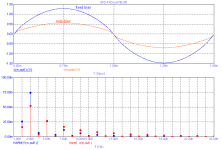
The problem with most auto bias circuits is that they modulate the bias voltage in such a way that the distortion will increase. Why this is becomes clear if we look at the voltage difference between input and output of the output stage. In my example comprising vertical MOSFETs. (BTW, the input voltage is defined as the mean value of the two gate voltages).
As can be seen from the figure below, the distortion with auto bias is clearly higher compared to fixed bias. At low frequencies no problem at all, as we have plenty of NFB loop gain to reduce the distortion to an acceptable level. At higher frequencies however, the NFB loop gain decreases and the additional distortion from the auto bias circuit will show up.
We can avoid this from happening by fixing the bias voltage for higher frequencies by means of a shunting capacitor across the bias circuit. BUT... there is one caveat: much change that the bias circuit will charge the capacitor to a higher level under dynamic conditions. This is because the average bias voltage (of most of such circuits) is higher than under idle conditions.
So, if we can manage that the capacitor will not be overcharged under dynamic conditions, then I see a bright future for auto bias circuits.
Cheers,
Edmond.
Simplex2 said:[snip]
This case (idle current stability in very low distortion amplifier) seems to be a dead end . The distortion modulation is negligible in a good design . This justifi the simple unperfect Vbe multiplier.
Hi Simplex,
While I agree with you that a simple Vbe multiplier does a fairly good job (see also my posts 3289 and 3297), I don't see an automatic bias circuit as a dead end (if that is what you are saying). Although it might not economic viable, I still think it's feasible and see it as a challenge to design a circuit that does not impair the THD figures in any way. Furthermore, this is DIY, so I don't care if it will cost a bit more than a simple Vbe multiplier.
The problem with most auto bias circuits is that they modulate the bias voltage in such a way that the distortion will increase. Why this is becomes clear if we look at the voltage difference between input and output of the output stage. In my example comprising vertical MOSFETs. (BTW, the input voltage is defined as the mean value of the two gate voltages).
As can be seen from the figure below, the distortion with auto bias is clearly higher compared to fixed bias. At low frequencies no problem at all, as we have plenty of NFB loop gain to reduce the distortion to an acceptable level. At higher frequencies however, the NFB loop gain decreases and the additional distortion from the auto bias circuit will show up.
We can avoid this from happening by fixing the bias voltage for higher frequencies by means of a shunting capacitor across the bias circuit. BUT... there is one caveat: much change that the bias circuit will charge the capacitor to a higher level under dynamic conditions. This is because the average bias voltage (of most of such circuits) is higher than under idle conditions.
So, if we can manage that the capacitor will not be overcharged under dynamic conditions, then I see a bright future for auto bias circuits.
Cheers,
Edmond.
Attachments
auto bias
Oops!
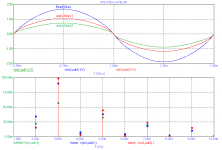
Sorry guys. My previous post contains an erroneous graph.
Here is the correct one, together with the results of a second auto bias circuit.
Blue: fixed bias voltage, Iq=140mA.
Red: LT1166 like auto bias, based on a constant product of the P- and N-source currents.
Green: auto bias, based on a nonlinear common control loop à la Marcel van de Gevel. This circuit prevents that if one the output devices is hard turned on, the other is completely turned off. Instead, it idles at a trickle current of ~10mA.
As one can see, the LT1166 like circuit produces less distortion at even harmonics, but at odd harmonics, which will dominate the THD figure, slightly more than the fixed bias circuit. Notice that I have not used a model of the LT1166 itself, rather a "function source" containing a mathematical expression that keeps the product of source currents constant.
The 2nd bias generator performs somewhere in between, but at the 3rd harmonic, clearly better. Notwithstanding that this circuit consumes 10-12 additional trannies, this one will probably be my favorite.
Cheers,
Edmond.
Oops!
Sorry guys. My previous post contains an erroneous graph.
Here is the correct one, together with the results of a second auto bias circuit.
Blue: fixed bias voltage, Iq=140mA.
Red: LT1166 like auto bias, based on a constant product of the P- and N-source currents.
Green: auto bias, based on a nonlinear common control loop à la Marcel van de Gevel. This circuit prevents that if one the output devices is hard turned on, the other is completely turned off. Instead, it idles at a trickle current of ~10mA.
As one can see, the LT1166 like circuit produces less distortion at even harmonics, but at odd harmonics, which will dominate the THD figure, slightly more than the fixed bias circuit. Notice that I have not used a model of the LT1166 itself, rather a "function source" containing a mathematical expression that keeps the product of source currents constant.
The 2nd bias generator performs somewhere in between, but at the 3rd harmonic, clearly better. Notwithstanding that this circuit consumes 10-12 additional trannies, this one will probably be my favorite.
Cheers,
Edmond.
Attachments
Re: auto bias
Hi Edmond,
Nice work! It is encouraging that the LT1166-like produces only slightly more THD than the fixed bias circuit, even at 3rd.
I wonder if the relative performance of these bias circuits, distortion-wise, changes depending on the nature of the matching between the models of the P and N channel devices.
Perhaps I missed it, but at what power level and into what impedance were these simulations run? Have you looked at these performances over a variety of power levels, especially at the power level where static crossover distortion is worst (which may be different for the different bias circuits)?
Thanks again.
Bob
Edmond Stuart said:Oops!
Sorry guys. My previous post contains an erroneous graph.
Here is the correct one, together with the results of a second auto bias circuit.
Blue: fixed bias voltage, Iq=140mA.
Red: LT1166 like auto bias, based on a constant product of the P- and N-source currents.
Green: auto bias, based on a nonlinear common control loop à la Marcel van de Gevel. This circuit prevents that if one the output devices is hard turned on, the other is completely turned off. Instead, it idles at a trickle current of ~10mA.
As one can see, the LT1166 like circuit produces less distortion at even harmonics, but at odd harmonics, which will dominate the THD figure, slightly more than the fixed bias circuit. Notice that I have not used a model of the LT1166 itself, rather a "function source" containing a mathematical expression that keeps the product of source currents constant.
The 2nd bias generator performs somewhere in between, but at the 3rd harmonic, clearly better. Notwithstanding that this circuit consumes 10-12 additional trannies, this one will probably be my favorite.
Cheers,
Edmond.
Hi Edmond,
Nice work! It is encouraging that the LT1166-like produces only slightly more THD than the fixed bias circuit, even at 3rd.
I wonder if the relative performance of these bias circuits, distortion-wise, changes depending on the nature of the matching between the models of the P and N channel devices.
Perhaps I missed it, but at what power level and into what impedance were these simulations run? Have you looked at these performances over a variety of power levels, especially at the power level where static crossover distortion is worst (which may be different for the different bias circuits)?
Thanks again.
Bob
Re: Re: auto bias
Thanks!
Hi Bob,
I think that the relative performance depends heavily on the Id/Vgs characteristics and matching as well.
As for the power level etc. you didn't miss anything, I forgot to mention it, sorry. It's 100W into 8 Ohm.
At 10W the figures change a bit: The THD of the LT-like circuit is twice the THD of the fixed bias output stage, while the THD of the Marcel-like bias is even three time higher.
Notice that these figures refer to the difference between input and output of the OPS and may not correlate with the final results of a complete amplifier. So, my next step will be simulating the distortion of just the output signal.
Also notice that the LT-like circuit is idealized. An accurate model of the LT1166 will probably give less favorable results.
Cheers,
Edmond.
Bob Cordell said:Hi Edmond,
Nice work!
Thanks!
It is encouraging that the LT1166-like produces only slightly more THD than the fixed bias circuit, even at 3rd.
I wonder if the relative performance of these bias circuits, distortion-wise, changes depending on the nature of the matching between the models of the P and N channel devices.
Perhaps I missed it, but at what power level and into what impedance were these simulations run? Have you looked at these performances over a variety of power levels, especially at the power level where static crossover distortion is worst (which may be different for the different bias circuits)?
Thanks again.
Bob
Hi Bob,
I think that the relative performance depends heavily on the Id/Vgs characteristics and matching as well.
As for the power level etc. you didn't miss anything, I forgot to mention it, sorry. It's 100W into 8 Ohm.
At 10W the figures change a bit: The THD of the LT-like circuit is twice the THD of the fixed bias output stage, while the THD of the Marcel-like bias is even three time higher.
Notice that these figures refer to the difference between input and output of the OPS and may not correlate with the final results of a complete amplifier. So, my next step will be simulating the distortion of just the output signal.
Also notice that the LT-like circuit is idealized. An accurate model of the LT1166 will probably give less favorable results.
Cheers,
Edmond.
auto bias
Hi Bob,
Now I have simulated the distortion in a different way: supplying an undistorted sine to the gates of the OPS, that is, keeping the mean value of the P-gate and the N-gate undistorted by means NFB, and then looking at distortion of the output signal (harmonics and THD as well).
At 1kHz and 10W into 8 Ohm, the fixed bias gives the best results (blue), then comes the LT-like bias (red), while the Marcel-like bias produces the most distortion. At 100W however, we get a different picture, see next post.
Attachments
auto bias
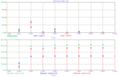
And here are the results at 100W. Now the Marcel-like bias is clearly the winner, followed by the fixed bias and then the LT-like bias.
Despite that the Marcel-like bias performs the worst at lower output levels (see previous figures), I still prefer this one, as the bias voltage is easily held constant at higher frequencies by means of a shunt capacitor . In doing so, the distortion is reduced to same level as for the fixed bias (see also post 3351).
Furthermore, the Marcel-like circuit is more flexible and compatible with lower Vgs-th MOSFETs, as low as 0.5V.
Cheers,
Edmond.
Attachments

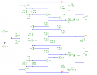
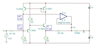
... coming back the topic of this thread: I have been participating in a dicussion in a French forum (as far as my feeble French allowed) about my ec amp as published in Elektor magazine. A member - Forr, who is also a member here - came up with a basic circuit that, in my view, nicely illustrated the concept. Offered here for whoever is interested.
Jan Didden
Jan Didden
Attachments
Thanks for sharing, Jan & Forr.
Helps a lot to understand the circuit with its error amplifier scheme and current style positive feedback.
BTW, even this simpified circuit performs quite well, I did a quick sim: Driving 10V into a 4R load, with the output buffer having 2R//schottky in series (heavy distortion mechanism, I'd say), it's only 0.5% (without the distortion network 0.0012%, as a reference). And without ec, some 15%.
- Klaus
EC
Hi Jan,
Hmm-- Essentially the same as:
http://www.diyaudio.com/forums/showthread.php?postid=1315310#post1315310
Do you see the difference?
Cheers,
Edmond.
janneman said:... coming back the topic of this thread: I have been participating in a dicussion in a French forum (as far as my feeble French allowed) about my ec amp as published in Elektor magazine. A member - Forr, who is also a member here - came up with a basic circuit that, in my view, nicely illustrated the concept. Offered here for whoever is interested.
Jan Didden
Hi Jan,
Hmm-- Essentially the same as:
http://www.diyaudio.com/forums/showthread.php?postid=1315310#post1315310
Do you see the difference?
Cheers,
Edmond.
Hi KSTR and Jan,
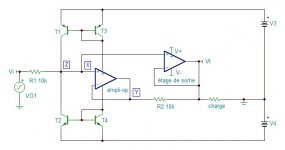
An even more simple circuit I later thought of. Anybody knowing what a current mirror is, how an op-amp works (the voltage at the inverting input is almost equal to the voltage at the non-inverting input) and that an output stage has a voltage gain not very linear and a bit lower than unity, is able to understand the error correction concept just applying the basic Ohm's law. Negative feedback is not so easy.
(translation : étage de sortie = output power stage; charge = load; ampli-op = op-amp)
Attachments
- Home
- Amplifiers
- Solid State
- Bob Cordell Interview: Error Correction