Distortion Performance
Hello Edmond
Looking THD wise it looks like the PGP amp is the best performing, is this correct. Has the PMP amp been built and tested and if so what THD specs does it achieve.
Just one question on the HEC output , the error amp Q7 and Q8 are mounted near the ouput devices does the Hawksford have a thermal issue, namely does bias current vary much with temperature after it is set. Is it safe to say its no worse than a Vbe multplier bias circuit.
Regards
Arthur
Re: Distortion Performance
Hawksford EC does not have any special thermal issues, output power devices may. Currently the PGP amp is build using lateral MOSFETs which do not need any thermal compensation. However, the PCB was designed to accept vertical MOSFET devices and bipolars. For these devices, thermal compensation is required and Q7/8 mounted on the HS are taking care of this.
On your other (first) question: it seems like you missed the whole point. Amps do not need to be built, measured and listened to, to confirm performance. Simulation is enough and anybody believing otherwise is a whining woman.
PHEONIX said:Hello Edmond
Looking THD wise it looks like the PGP amp is the best performing, is this correct. Has the PMP amp been built and tested and if so what THD specs does it achieve.
Just one question on the HEC output , the error amp Q7 and Q8 are mounted near the ouput devices does the Hawksford have a thermal issue, namely does bias current vary much with temperature after it is set. Is it safe to say its no worse than a Vbe multplier bias circuit.
Regards
Arthur
Hawksford EC does not have any special thermal issues, output power devices may. Currently the PGP amp is build using lateral MOSFETs which do not need any thermal compensation. However, the PCB was designed to accept vertical MOSFET devices and bipolars. For these devices, thermal compensation is required and Q7/8 mounted on the HS are taking care of this.
On your other (first) question: it seems like you missed the whole point. Amps do not need to be built, measured and listened to, to confirm performance. Simulation is enough and anybody believing otherwise is a whining woman.
Re: Distortion Performance
Hi Arthur,
The PGP amp has been built and tested already, while the PMP amp is still in the design/simulation and phase. Although the simulation results a very promising (and better), real life measurements (and listening test, for what they are worth) has to be done first, before I can say hurray.
Regarding thermal issues, I don't think there are serious problems, although it should be noticed that the bias voltage depends a bit more on the current through Q7 and Q8 compared to a traditional Vbe multiplier (and even more WRT an enhanced version of the latter, also invented by Hawksford). This is because of the emitter series resistors of Q7 and Q8 lower the gain, or as you like, increase the effective/equivalent output impedance of the bias circuit.
Cheers,
Edmond.
PHEONIX said:Hello Edmond
Looking THD wise it looks like the PGP amp is the best performing, is this correct. Has the PMP amp been built and tested and if so what THD specs does it achieve.
Just one question on the HEC output , the error amp Q7 and Q8 are mounted near the ouput devices does the Hawksford have a thermal issue, namely does bias current vary much with temperature after it is set. Is it safe to say its no worse than a Vbe multplier bias circuit.
Regards
Arthur
Hi Arthur,
The PGP amp has been built and tested already, while the PMP amp is still in the design/simulation and phase. Although the simulation results a very promising (and better), real life measurements (and listening test, for what they are worth) has to be done first, before I can say hurray.
Regarding thermal issues, I don't think there are serious problems, although it should be noticed that the bias voltage depends a bit more on the current through Q7 and Q8 compared to a traditional Vbe multiplier (and even more WRT an enhanced version of the latter, also invented by Hawksford). This is because of the emitter series resistors of Q7 and Q8 lower the gain, or as you like, increase the effective/equivalent output impedance of the bias circuit.
Cheers,
Edmond.
Edmond Stuart said:
BTW, opposed to what some touchy people here apparently think, I have nothing against the LT1166 <snip>
You promised some detailed results on your simulations using the LT1166. Because you are so open to analyzing new circuits and concepts, ultimately have nothing against this IC, and complained about the device model, I have decided to help you in your endeavour of proving your point(s) and publish the detailed schematic of this IC internals (minus some non-essential, diode based, protection circuitry).
http://www.synaesthesia.ca/files/LT1166.PNG
From this point, anybody can pick up and experiment (by simulation or by breadboarding) various configuration using this IC (and God knows, it can be used in quite some). The P and N devices models are not critical, you can use the ones in the model I have published above:
.model NP NPN(BF=125 Cje=.5p Cjc=.5p Rb=500)
.model PN PNP(BF=125 Cje=.5p Cjc=.5p Rb=500)
The number across each tranny is the device area. It is important to specify this parameter for each tranny, otherwise nothing will work properly.
If your busy schedule will accomodate this small piece of work, I am sure everybody will appreciate.
You are welcomed 😀
syn08 said:
A word to the wise, I've mentioned this before. If you think you want to actually financially benefit from your work don't publish unpatented schematics. Once you publish the schematic you have given away the store. Legally those disclaimers like "not for commercial use" are worth nada, zero. Speaking for the States of course.
scott wurcer said:A word to the wise, I've mentioned this before. If you think you want to actually financially benefit from your work don't publish unpatented schematics. Once you publish the schematic you have given away the store. Legally those disclaimers like "not for commercial use" are worth nada, zero. Speaking for the States of course.
Thanks Scott, wise advice. I thought for a second I'm going to be rich. Then I woke up 😀
LT1166
I've already "proved" my point, see: http://www.diyaudio.com/forums/showthread.php?postid=1479734#post1479734
This simulation was based on a simple mathematical expression that mimics the bias generator of the LT1166.
Besides, some experts share my opinion that a fixed bias voltage gives less distortion.
Last but not least, mark your own words:
EOD
syn08 said:You promised some detailed results on your simulations using the LT1166.
[snip]
If your busy schedule will accomodate this small piece of work, I am sure everybody will appreciate.
You are welcomed 😀 [/B]
I've already "proved" my point, see: http://www.diyaudio.com/forums/showthread.php?postid=1479734#post1479734
This simulation was based on a simple mathematical expression that mimics the bias generator of the LT1166.
Besides, some experts share my opinion that a fixed bias voltage gives less distortion.
Last but not least, mark your own words:
syn08 said:Given the circumstances, I do not wish to further pursue this debate. Please accept my excuses and discard my rather cryptic comment.
[snip]
EOD
scott wurcer said:A word to the wise, I've mentioned this before. If you think you want to actually financially benefit from your work don't publish unpatented schematics. Once you publish the schematic you have given away the store. Legally those disclaimers like "not for commercial use" are worth nada, zero. Speaking for the States of course.
Hi Scott,
One of the reasons I make my schematics public is to prevent that others apply for a patent based on my tricks (of course, as long as these tricks are patentable at all).
Cheers,
Edmond.
LT1166 vs Vbe multiplier
Hi Bob,
I ask you a couple of days ago if you have any idea of the max. temperature difference one might expect between the junctions of the output devices and the Vbe multiplier.
Apparently, you have overlooked my post. Never mind. In the mean time I've figured it out myself.
Suppose we have a 100W amp, supply voltage = +/- 50V, Iq = 150mA and RL = 8 Ohm (resistive).
Then the min. and max. power dissipation per device is about 7.5 respectively 32.5W. This means a difference of 25W.
Next, suppose that the thermal resistance of junction to case is 0.7dgr/W, then the max. thermal mismatch between an output device and the Vbe multiplier is 25*0.7=17.5dgr.
Given a tempco of about 4mV/dgr for vertical MOSFETs, this will result in a bias error of 17.5*4 = 70mV.
One of my NFB output stages produces a THD20=34ppm at the correct bias voltage (see post 3260).
If I decrease Vbias by 140mV, I get 37ppm,
and if I increase Vbias 140mV, I get 34ppm.
An ideal model of the LT1166 on the other hand, raises the THD20 to 103ppm. So I guess you will not be surprised if I give up to implement this chip in my design.
Please, notice that these figures only apply to a particular set of 2SJ201/2SK1530 that I have purchased. Using other devices may, of course, result in different figures.
Cheers,
Edmond.
Bob Cordell said:..........
It does not just prevent thermal runaway, but also reduces the impact of fast-changing junction temperatures under program conditions that can lead to an output stage being way sub-optimally biased on a dynamic basis.
.............
Cheers,
Bob
Hi Bob,
I ask you a couple of days ago if you have any idea of the max. temperature difference one might expect between the junctions of the output devices and the Vbe multiplier.
Apparently, you have overlooked my post. Never mind. In the mean time I've figured it out myself.
Suppose we have a 100W amp, supply voltage = +/- 50V, Iq = 150mA and RL = 8 Ohm (resistive).
Then the min. and max. power dissipation per device is about 7.5 respectively 32.5W. This means a difference of 25W.
Next, suppose that the thermal resistance of junction to case is 0.7dgr/W, then the max. thermal mismatch between an output device and the Vbe multiplier is 25*0.7=17.5dgr.
Given a tempco of about 4mV/dgr for vertical MOSFETs, this will result in a bias error of 17.5*4 = 70mV.
One of my NFB output stages produces a THD20=34ppm at the correct bias voltage (see post 3260).
If I decrease Vbias by 140mV, I get 37ppm,
and if I increase Vbias 140mV, I get 34ppm.
An ideal model of the LT1166 on the other hand, raises the THD20 to 103ppm. So I guess you will not be surprised if I give up to implement this chip in my design.
Please, notice that these figures only apply to a particular set of 2SJ201/2SK1530 that I have purchased. Using other devices may, of course, result in different figures.
Cheers,
Edmond.
syn08 said:
You promised some detailed results on your simulations using the LT1166. Because you are so open to analyzing new circuits and concepts, ultimately have nothing against this IC, and complained about the device model, I have decided to help you in your endeavour of proving your point(s) and publish the detailed schematic of this IC internals (minus some non-essential, diode based, protection circuitry).
http://www.synaesthesia.ca/files/LT1166.PNG
From this point, anybody can pick up and experiment (by simulation or by breadboarding) various configuration using this IC (and God knows, it can be used in quite some). The P and N devices models are not critical, you can use the ones in the model I have published above:
.model NP NPN(BF=125 Cje=.5p Cjc=.5p Rb=500)
.model PN PNP(BF=125 Cje=.5p Cjc=.5p Rb=500)
The number across each tranny is the device area. It is important to specify this parameter for each tranny, otherwise nothing will work properly.
If your busy schedule will accomodate this small piece of work, I am sure everybody will appreciate.
You are welcomed 😀
Thanks for your effort and contribution here.
Bob
Re: LT1166 vs Vbe multiplier
Thanks God you haven't attempted to implement in real life an OPS with LT1166 and 2SK1530/2SJ201. You would have a very nasty surprise to not have it working (not even as in the datasheet applications), or even worse, to blow the rather expensive MOSFET devices you just purchased.
Why? I'll save you a question and let you know that LT1166 needs at least about 4 volts across pins 1 and 4 to work properly. Your pair would allow not even 2 volts and at that voltage the LT1166 won't be able to keep the voltage across the source resistors constant at 20mV. KABOOM! 😀
Speaking about differences between simulation and real life...
Edmond Stuart said:
Hi Bob,
I ask you a couple of days ago if you have any idea of the max. temperature difference one might expect between the junctions of the output devices and the Vbe multiplier.
Apparently, you have overlooked my post. Never mind. In the mean time I've figured it out myself.
Suppose we have a 100W amp, supply voltage = +/- 50V, Iq = 150mA and RL = 8 Ohm (resistive).
Then the min. and max. power dissipation per device is about 7.5 respectively 32.5W. This means a difference of 25W.
Next, suppose that the thermal resistance of junction to case is 0.7dgr/W, then the max. thermal mismatch between an output device and the Vbe multiplier is 25*0.7=17.5dgr.
Given a tempco of about 4mV/dgr for vertical MOSFETs, this will result in a bias error of 17.5*4 = 70mV.
One of my NFB output stages produces a THD20=34ppm at the correct bias voltage (see post 3260).
If I decrease Vbias by 140mV, I get 37ppm,
and if I increase Vbias 140mV, I get 34ppm.
An ideal model of the LT1166 on the other hand, raises the THD20 to 103ppm. So I guess you will not be surprised if I give up to implement this chip in my design.
Please, notice that these figures only apply to a particular set of 2SJ201/2SK1530 that I have purchased. Using other devices may, of course, result in different figures.
Cheers,
Edmond.
Thanks God you haven't attempted to implement in real life an OPS with LT1166 and 2SK1530/2SJ201. You would have a very nasty surprise to not have it working (not even as in the datasheet applications), or even worse, to blow the rather expensive MOSFET devices you just purchased.
Why? I'll save you a question and let you know that LT1166 needs at least about 4 volts across pins 1 and 4 to work properly. Your pair would allow not even 2 volts and at that voltage the LT1166 won't be able to keep the voltage across the source resistors constant at 20mV. KABOOM! 😀
Speaking about differences between simulation and real life...
Re: LT1166 vs Vbe multiplier
Hi Edmond,
I apologize for not getting back to you sooner.
What you have described seems to be a pretty good way to look at the problem. I would put in a couple of different numbers and some caveats, however.
First, I've often seen closer to 6 mV/C for vertical MOSFET Vgs tempco.
Second, you should probably include the thermal resistance of the transistor's mounting insulator, perhaps an additional 0.5C/W.
If you do this, you now get 6 mV/C * 1.2C/W * 25W = 180 mV.
With transconductance on the order of 0.6S at a bias of 150 mA, this could theoretically result in a bias shift of over 100 mA, possibly under-biasing the MOSFET right after a high-dissipation interval.
With an output stage using error correction or something equivalent, the circuit may very well do OK on distortion rise on such a reduced bias (one of the main reasons I applied HEC to vertical MOSFETs in 1983). However, in a more conventional MOSFET power amplifier, the resultant distortion rise might be quite objectionable.
Finally, note that, as I illustrated in my MOSFET EC amplifier paper, this kind of bias behavior is a much greater problem with bipolar output stages.
Cheers,
Bob
Edmond Stuart said:
Hi Bob,
I ask you a couple of days ago if you have any idea of the max. temperature difference one might expect between the junctions of the output devices and the Vbe multiplier.
Apparently, you have overlooked my post. Never mind. In the mean time I've figured it out myself.
Suppose we have a 100W amp, supply voltage = +/- 50V, Iq = 150mA and RL = 8 Ohm (resistive).
Then the min. and max. power dissipation per device is about 7.5 respectively 32.5W. This means a difference of 25W.
Next, suppose that the thermal resistance of junction to case is 0.7dgr/W, then the max. thermal mismatch between an output device and the Vbe multiplier is 25*0.7=17.5dgr.
Given a tempco of about 4mV/dgr for vertical MOSFETs, this will result in a bias error of 17.5*4 = 70mV.
One of my NFB output stages produces a THD20=34ppm at the correct bias voltage (see post 3260).
If I decrease Vbias by 140mV, I get 37ppm,
and if I increase Vbias 140mV, I get 34ppm.
An ideal model of the LT1166 on the other hand, raises the THD20 to 103ppm. So I guess you will not be surprised if I give up to implement this chip in my design.
Please, notice that these figures only apply to a particular set of 2SJ201/2SK1530 that I have purchased. Using other devices may, of course, result in different figures.
Cheers,
Edmond.
Hi Edmond,
I apologize for not getting back to you sooner.
What you have described seems to be a pretty good way to look at the problem. I would put in a couple of different numbers and some caveats, however.
First, I've often seen closer to 6 mV/C for vertical MOSFET Vgs tempco.
Second, you should probably include the thermal resistance of the transistor's mounting insulator, perhaps an additional 0.5C/W.
If you do this, you now get 6 mV/C * 1.2C/W * 25W = 180 mV.
With transconductance on the order of 0.6S at a bias of 150 mA, this could theoretically result in a bias shift of over 100 mA, possibly under-biasing the MOSFET right after a high-dissipation interval.
With an output stage using error correction or something equivalent, the circuit may very well do OK on distortion rise on such a reduced bias (one of the main reasons I applied HEC to vertical MOSFETs in 1983). However, in a more conventional MOSFET power amplifier, the resultant distortion rise might be quite objectionable.
Finally, note that, as I illustrated in my MOSFET EC amplifier paper, this kind of bias behavior is a much greater problem with bipolar output stages.
Cheers,
Bob
Re: Re: LT1166 vs Vbe multiplier

Do you really think I'm that stupid?
PS: After 3 months, I'm still waiting for H(s) of the NFB-OPS.
syn08 said:Thanks God you haven't attempted to implement in real life an OPS with LT1166 and 2SK1530/2SJ201. You would have a very nasty surprise to not have it working (not even as in the datasheet applications), or even worse, to blow the rather expensive MOSFET devices you just purchased.
Why? I'll save you a question and let you know that LT1166 needs at least about 4 volts across pins 1 and 4 to work properly. Your pair would allow not even 2 volts and at that voltage the LT1166 won't be able to keep the voltage across the source resistors constant at 20mV. KABOOM! 😀
Speaking about differences between simulation and real life...
Do you really think I'm that stupid?
PS: After 3 months, I'm still waiting for H(s) of the NFB-OPS.
Re: Re: Re: LT1166 vs Vbe multiplier
I'm sorry, but you did not hold your breath 😀
P.S. I'm pretty sure you are not stupid enough to touch a breadboard. That's for stupid mortals not for Simulation Gods.
Edmond Stuart said:
PS: After 3 months, I'm still waiting for H(s) of the NFB-OPS.
I'm sorry, but you did not hold your breath 😀
P.S. I'm pretty sure you are not stupid enough to touch a breadboard. That's for stupid mortals not for Simulation Gods.
Btw regarding this LT1166, I just had the idea to misuse it to hold the power constant in an output transistor. Would be doable especially with a cascode: the LT controlling cascode voltage in order to hold Vds*Id constant (at least on a time averaged level). Id could be sensed in the drain lead of the main FET (for D2S biasing). Overall bias current would still be controlled by a standard external Vbe-mult. One would need to cheat a little to keep the voltage in bound (and the LT in closed loop) when current is totally cut off. Not sure if the effects of Vds modulation, depending how quick one would choose the loop to react, would spoil the whole approach. But at least it would keep things thermally stable but maintaining freedom of choice for the actual biasing.
- Klaus
- Klaus
This is one of the clever ways to use this circuit. I've tried something similar and indeed it works very good. Even more/better can be done, however the complexity starts to increase to the point it's not anymore worth of.
Re: Re: LT1166 vs Vbe multiplier
No problem at all. I suppose you had more important things to do.
Thanks for the tip.
Hi Bob,
I substituted +/- 180mV.
At -180mV I get THD20=40.5ppm
At +180mV I get THD20=34.3ppm
Not that bad, don't you think so?
Regarding BJTs, you're absolute right. These kind of trannies are much more sensitive to bias errors.
As for the Vgs tempco of MOSFETs, in your paper you mentioned 5mV/C. Any idea where to get more info on this topic?
Cheers,
Edmond.
Bob Cordell said:Hi Edmond,
I apologize for not getting back to you sooner.
No problem at all. I suppose you had more important things to do.
What you have described seems to be a pretty good way to look at the problem. I would put in a couple of different numbers and some caveats, however.
First, I've often seen closer to 6 mV/C for vertical MOSFET Vgs tempco.
Thanks for the tip.
Second, you should probably include the thermal resistance of the transistor's mounting insulator, perhaps an additional 0.5C/W.
If you do this, you now get 6 mV/C * 1.2C/W * 25W = 180 mV.
With transconductance on the order of 0.6S at a bias of 150 mA, this could theoretically result in a bias shift of over 100 mA, possibly under-biasing the MOSFET right after a high-dissipation interval.
With an output stage using error correction or something equivalent, the circuit may very well do OK on distortion rise on such a reduced bias (one of the main reasons I applied HEC to vertical MOSFETs in 1983). However, in a more conventional MOSFET power amplifier, the resultant distortion rise might be quite objectionable.
Finally, note that, as I illustrated in my MOSFET EC amplifier paper, this kind of bias behavior is a much greater problem with bipolar output stages.
Cheers,
Bob
Hi Bob,
I substituted +/- 180mV.
At -180mV I get THD20=40.5ppm
At +180mV I get THD20=34.3ppm
Not that bad, don't you think so?
Regarding BJTs, you're absolute right. These kind of trannies are much more sensitive to bias errors.
As for the Vgs tempco of MOSFETs, in your paper you mentioned 5mV/C. Any idea where to get more info on this topic?
Cheers,
Edmond.
Re: Re: Re: LT1166 vs Vbe multiplier
Being strictly voltage controlled devices, MOSFETs do not usually have any Vgs tempco directly specified as a datasheet parameter. This is the same kind of reasoning why a bipolar device does not have defined an explicit base current tempco (but, in this case, a Vbe tempco). A Vgs tempco could implicitly be defined as "the voltage variation required to keept the drain current constant, for a 1 degree of temperature variation", but usually it is the Id that it's considered as having a tempco.
Now, switching MOSFET users couldn't care less for any Id tempco, so even that is usually not specified. The very few MOSFETs intended for analog applications (including the 2SK1530) have the Id-Vgs with temp as a parameter plotted in the datasheet. You can define your own Vgs tempco from there, if that fits you better.
Edmond Stuart said:
As for the Vgs tempco of MOSFETs, in your paper you mentioned 5mV/C.
Being strictly voltage controlled devices, MOSFETs do not usually have any Vgs tempco directly specified as a datasheet parameter. This is the same kind of reasoning why a bipolar device does not have defined an explicit base current tempco (but, in this case, a Vbe tempco). A Vgs tempco could implicitly be defined as "the voltage variation required to keept the drain current constant, for a 1 degree of temperature variation", but usually it is the Id that it's considered as having a tempco.
Now, switching MOSFET users couldn't care less for any Id tempco, so even that is usually not specified. The very few MOSFETs intended for analog applications (including the 2SK1530) have the Id-Vgs with temp as a parameter plotted in the datasheet. You can define your own Vgs tempco from there, if that fits you better.
Re: Re: Re: Re: LT1166 vs Vbe multiplier
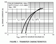
The good old IRFP240 shown has, at 100mA, about 0.9V delta Vgs from 25degC to 150degC, which gives the claimed figure for this device class of about 7mV/degC.
- Klaus
EDIT: Typos
Not a single valued parameter, but indirectly as the transfer characteristic at different temperatures, which allows us to get the Vgs tempco at a given drain current. Problem often is that these curves stop at way to high currents, but in most datasheets even for switching devices, the graph is shown at least.syn08 said:Being strictly voltage controlled devices, MOSFETs do not usually have any Vgs tempco directly specified as a datasheet parameter.
The good old IRFP240 shown has, at 100mA, about 0.9V delta Vgs from 25degC to 150degC, which gives the claimed figure for this device class of about 7mV/degC.
- Klaus
EDIT: Typos
Attachments
Re: Re: Re: Re: Re: LT1166 vs Vbe multiplier
That's what I am saying. It doesn't make much sense to talk about Vgs tempco, as long as Vgs cannot really move around with temperature. Id can and does.
Moreover, the Id tempco depends on Id itself (and the zero tempco is in the amps range for verticals, much lower for laterals, etc...) so one more reason not to specify this in a data sheet other than a Id-Vgs curve. I agree that these curves are usually around high currents.
Finally, at low currents, the "Vgs tempco" is essentialy determined by the MOSFET threshod voltage variation with temperature. Id~(Vgs-Vt)^2 therefore the "Vgs tempco" is equal to the Vt tempco (and is of course negative). Unfortunately, the Vt tempco depends on lots of variables, most of them significantly related to the manufacturing technology and device layout (HEXFETs from IR are different than STRIPFETs from ST). Therefore, the Vt tempco is barely consistent across similar devices coming from various manufacturers. This is another good reason why a design should not rely on a precise Vgs tempco at low currents.
In another life, I've measured tempcos as low as 2.5mV/C and as high as 6.2mV/C. For example the OnSemi's NTLJS3113P has a Vth tempco specified (and measured) at typ 2.68mV/C but this is a rather low power device. One to another, a 5 to 6mV/C tempco is kinda worst case. 4-5mV/C would be, say, typical for modern, medium power devices.
Edit: IRF240/IRF9240 do not qualify as "modern devices", and in general none of the IRF classics do. Fairchild, OnSemi and in particular ST are really modern devices. Look at the ST STB19NF20, the Vth coefficient is typically under 5mV/C and that's a 19A 200V device. OTOH, the STP17NK40Z (400V and 17A) has a Vth tempco of about 7mV/C.
KSTR said:
Not a single valued parameter, but indirectly as the transfer characteristic at different temperatures, which allows us to get the Vgs tempco at a given drain current.
That's what I am saying. It doesn't make much sense to talk about Vgs tempco, as long as Vgs cannot really move around with temperature. Id can and does.
Moreover, the Id tempco depends on Id itself (and the zero tempco is in the amps range for verticals, much lower for laterals, etc...) so one more reason not to specify this in a data sheet other than a Id-Vgs curve. I agree that these curves are usually around high currents.
Finally, at low currents, the "Vgs tempco" is essentialy determined by the MOSFET threshod voltage variation with temperature. Id~(Vgs-Vt)^2 therefore the "Vgs tempco" is equal to the Vt tempco (and is of course negative). Unfortunately, the Vt tempco depends on lots of variables, most of them significantly related to the manufacturing technology and device layout (HEXFETs from IR are different than STRIPFETs from ST). Therefore, the Vt tempco is barely consistent across similar devices coming from various manufacturers. This is another good reason why a design should not rely on a precise Vgs tempco at low currents.
In another life, I've measured tempcos as low as 2.5mV/C and as high as 6.2mV/C. For example the OnSemi's NTLJS3113P has a Vth tempco specified (and measured) at typ 2.68mV/C but this is a rather low power device. One to another, a 5 to 6mV/C tempco is kinda worst case. 4-5mV/C would be, say, typical for modern, medium power devices.
Edit: IRF240/IRF9240 do not qualify as "modern devices", and in general none of the IRF classics do. Fairchild, OnSemi and in particular ST are really modern devices. Look at the ST STB19NF20, the Vth coefficient is typically under 5mV/C and that's a 19A 200V device. OTOH, the STP17NK40Z (400V and 17A) has a Vth tempco of about 7mV/C.
- Home
- Amplifiers
- Solid State
- Bob Cordell Interview: Error Correction