Re: Re: Re: Re: Re: Re: Re: LT1166
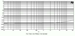
I tried it both ways. I set up a MOSFET follower stage and drove
pin 2 as shown in the app notes Fig 1, and I got a curve comparable
to the one they showed, which at 1 watt is maybe .1% at low
frequencies climbing rapidly above 10k or so.
I also drove it as you did through pins 1 and 4 with pin 2 floating,
and for open loop I got similar results.
Perhaps I was doing something wrong, but I can't imagine what it
might have been. As I said before, I played around with it for a
couple of days, trying to do better.
If you know me at all, you understand that I'm not particularly hung
up about distortion numbers, but below you can see the open loop
figure for the output stage in question.
Clearly I was doing better with just a fixed bias. Since the chip
seems to work for you, I'll give it another shot sometime.
syn08 said:Do you remeber some numbers? How much HF distortions you got with the LT1166?
The data sheet has some distortion information, but only for the transconductance stage, that myself (and, as far as I understand, yourself) did not use.
I tried it both ways. I set up a MOSFET follower stage and drove
pin 2 as shown in the app notes Fig 1, and I got a curve comparable
to the one they showed, which at 1 watt is maybe .1% at low
frequencies climbing rapidly above 10k or so.
I also drove it as you did through pins 1 and 4 with pin 2 floating,
and for open loop I got similar results.
Perhaps I was doing something wrong, but I can't imagine what it
might have been. As I said before, I played around with it for a
couple of days, trying to do better.
If you know me at all, you understand that I'm not particularly hung
up about distortion numbers, but below you can see the open loop
figure for the output stage in question.
Clearly I was doing better with just a fixed bias. Since the chip
seems to work for you, I'll give it another shot sometime.
Attachments
Re: Re: LT1166
Of course it has an effect. Now, try and float the V/I stage over the amp output as in my last schematic. You'll have a nice surprise even in simulations. Then ask your simulator why this can be a problem in the real world and what can be done about.
Edmond Stuart said:
Huh? Modulation of Vbias has definitely an effect on the transmission, because it alters the gm of the output stage.
Here some figures from my "armchair":
Circuit: NFB output stage
Devices: 2SJ201/2SK1530
Iq = 150mA
Po=50W in 8 Ohm
With fixed Vbias THD20=34ppm
With fixed Id product THD20=103ppm
Cheers, Edmond.
Of course it has an effect. Now, try and float the V/I stage over the amp output as in my last schematic. You'll have a nice surprise even in simulations. Then ask your simulator why this can be a problem in the real world and what can be done about.
Re: Re: LT1166
Hi Edmond,
Please note that I said "transmission TO the output stage".
Modulation of the bias certainly DOES have an effect on the total gm of the output complementary pair.
Cheers,
Bob
Edmond Stuart said:
Huh? Modulation of Vbias has definitely an effect on the transmission, because it alters the gm of the output stage.
Here some figures from my "armchair":
Circuit: NFB output stage
Devices: 2SJ201/2SK1530
Iq = 150mA
Po=50W in 8 Ohm
With fixed Vbias THD20=34ppm
With fixed Id product THD20=103ppm
Cheers, Edmond.
Hi Edmond,
Please note that I said "transmission TO the output stage".
Modulation of the bias certainly DOES have an effect on the total gm of the output complementary pair.
Cheers,
Bob
Re: Re: Re: LT1166
What do you mean by: "try and float the V/I stage over the amp output ". Could you be a bit more specific?
Also, please, could you send me the your last schematic to make sure we are talking about the same circuit.
syn08 said:Of course it has an effect. Now, try and float the V/I stage over the amp output as in my last schematic. You'll have a nice surprise even in simulations. Then ask your simulator why this can be a problem in the real world and what can be done about.
What do you mean by: "try and float the V/I stage over the amp output ". Could you be a bit more specific?
Also, please, could you send me the your last schematic to make sure we are talking about the same circuit.
Re: Re: Re: LT1166
Hi Bob,
You are perfectly right. I'm sorry I've overlooked this small but important subtlety. Sometimes, "to" and "of" make a big difference.
BTW, what do you think about my THD figures, encouraging or disappointing?
Cheers, Edmond.
Bob Cordell said:Hi Edmond,
Please note that I said "transmission TO the output stage".
Modulation of the bias certainly DOES have an effect on the total gm of the output complementary pair.
Cheers,
Bob
Hi Bob,
You are perfectly right. I'm sorry I've overlooked this small but important subtlety. Sometimes, "to" and "of" make a big difference.
BTW, what do you think about my THD figures, encouraging or disappointing?
Cheers, Edmond.
Re: Re: Re: Re: LT1166
Please provide your current schematic and the LT1166 model you are currently using.
Otherwise, lacking any experimental/measurements data on your side, at least the simulations should be calibrated and aligned to allow any further comparisons or discussions.
Edmond Stuart said:
What do you mean by: "try and float the V/I stage over the amp output ". Could you be a bit more specific?
Also, please, could you send me the your last schematic to make sure we are talking about the same circuit.
Please provide your current schematic and the LT1166 model you are currently using.
Otherwise, lacking any experimental/measurements data on your side, at least the simulations should be calibrated and aligned to allow any further comparisons or discussions.
Re: Re: Re: Re: Re: LT1166
Apart from not answering my question, it's not a good idea -at this moment- to show my latest version of the NFB-OPS here, as it will raise more questions than answers. In a couple of weeks, I will put the schematic plus explanation on my website.
So let's turn back to your previous remark:
"Now, try and float the V/I stage over the amp output as in my last schematic. You'll have a nice surprise even in simulations."
I ask you again, what do you mean by "float", which "V/I stage" and which "last schematic".
Also, why don't tell us right now what that "surprise" is all about.
syn08 said:Please provide your current schematic and the LT1166 model you are currently using.
Otherwise, lacking any experimental/measurements data on your side, at least the simulations should be calibrated and aligned to allow any further comparisons or discussions.
Apart from not answering my question, it's not a good idea -at this moment- to show my latest version of the NFB-OPS here, as it will raise more questions than answers. In a couple of weeks, I will put the schematic plus explanation on my website.
So let's turn back to your previous remark:
"Now, try and float the V/I stage over the amp output as in my last schematic. You'll have a nice surprise even in simulations."
I ask you again, what do you mean by "float", which "V/I stage" and which "last schematic".
Also, why don't tell us right now what that "surprise" is all about.
Re: Re: Re: Re: Re: Re: LT1166
Given the circumstances, I do not wish to further pursue this debate. Please accept my excuses and discard my rather cryptic comment.
Good luck with your new design.
Given the circumstances, I do not wish to further pursue this debate. Please accept my excuses and discard my rather cryptic comment.
Good luck with your new design.
Re: LT1166
Because the PGP project has been finished and you don't need me any longer????
I accept your excuses and discard your rather cryptic comment, together with the other posts.
Thank you so much!
syn08 said:Given the circumstances, I do not wish to further pursue this debate.
Because the PGP project has been finished and you don't need me any longer????
Please accept my excuses and discard my rather cryptic comment.
I accept your excuses and discard your rather cryptic comment, together with the other posts.
Good luck with your new design.
Thank you so much!
Re: LT1166
Hi Bob,
In order to estimate the impact of fast-changing junction temperatures (due to thermal delay), do you have any idea of the max. temperature difference one might expect between the junctions of the output devices and the Vbe multiplier?
Also, how large is the thermal time constant inside a typical OP device? About 1ms?
Cheers, Edmond.
Bob Cordell said:It does not just prevent thermal runaway, but also reduces the impact of fast-changing junction temperatures under program conditions that can lead to an output stage being way sub-optimally biased on a dynamic basis.
[snip]
Cheers,
Bob
Hi Bob,
In order to estimate the impact of fast-changing junction temperatures (due to thermal delay), do you have any idea of the max. temperature difference one might expect between the junctions of the output devices and the Vbe multiplier?
Also, how large is the thermal time constant inside a typical OP device? About 1ms?
Cheers, Edmond.
Thermal response includes chip, encapsulation, metal tab thermal capacities and thermal resistance
I'm sure papers with detailed modeling can be found
lazy engineers would just point to the
"THERMAL RESPONSE JUNCTION TO CASE
vs
POWER PULSE DURATION"
graphs sometimes found on power transistor datasheets
from the graph for a large MOSFET I see 10-100mS pulse widths span 20-50% "ZθJC / RθJC - Normalised Transient Thermal Impedance" for low duty pulses
a "intelligent" bias circuit is certainly possible today with AVR/MSP430/PIC uC chips with 10-12 bit ADC going for a few $ ea, complete demo dev environments for < $50
monitor device I*V, identify thermal model with Vbe and/or other Temp sensor, use DAC or filtered PWM output for bias V, could include SOA, current limit, DC offset protection (with relay) functions
Hi JCX,
Thanks for the response. However, you didn't (precisely) answered my two questions. I need these answers in order to compare the degradation (in terms of THD) caused by the LT1166 vs the degradation caused thermal delay of the classical Vbe multiplier mounted on the heat sink.
NB: Please don't misunderstand my reply. Your suggestions are quite valuable, but at this moment, I need a clear picture of the pro and cons of a simple Vbe multiplier.
Cheers, Edmond.
Hey Edmond, how about a "My retaliation against the LT1166" page addition to your website, like this one by a guy who doesn't like PIC's:
http://members.ozemail.com.au/~bobpar/pichate.htm
😀 😀
http://members.ozemail.com.au/~bobpar/pichate.htm
😀 😀
G.Kleinschmidt said:Hey Edmond, how about a "My retaliation against the LT1166" page addition to your website, like this one by a guy who doesn't like PIC's:
http://members.ozemail.com.au/~bobpar/pichate.htm
😀 😀

BTW, opposed to what some touchy people here apparently think, I have nothing against the LT1166, but if I find something that produces less distortion, even it's meager few percent and even it's a bit more expensive, I opt for that.
Cheers, Edmond
Edmond Stuart said:
but if I find something that produces less distortion, even it's meager few percent and even it's a bit more expensive, I opt for that.
A very good strategy, in particular when you don't have to build anything, or pick the bill 😀. Let those touchy people think about costs and cost/performance analysis.
Error correction using bipolars
Hello Edmond
With your very lowTHD amp circuits how low is the THD when you use bipolar ouput transistors. Do they achieve 1ppm thd a20Khz like I presume the Fets do.
Regards
Arthur
Hello Edmond
With your very lowTHD amp circuits how low is the THD when you use bipolar ouput transistors. Do they achieve 1ppm thd a20Khz like I presume the Fets do.
Regards
Arthur
Re: Error correction using bipolars
Hi Arthur,
At the moment, I don't know exactly. Generally, this means a complete redesign and checking all FB loops all over again. But I guess equal or even better THD figures.
BTW, you're not the only one who ask me this question. When time allows, I'll simulate such configuration, for what it is worth.
I'll hope I haven't disappointed you too much with this vague guess.
Cheers,
Edmond.
PS: Which amp do you exactly mean: PGP or PMP?
PHEONIX said:Hello Edmond
With your very low THD amp circuits how low is the THD when you use bipolar ouput transistors. Do they achieve 1ppm thd a20Khz like I presume the Fets do.
Regards
Arthur
Hi Arthur,
At the moment, I don't know exactly. Generally, this means a complete redesign and checking all FB loops all over again. But I guess equal or even better THD figures.
BTW, you're not the only one who ask me this question. When time allows, I'll simulate such configuration, for what it is worth.
I'll hope I haven't disappointed you too much with this vague guess.
Cheers,
Edmond.
PS: Which amp do you exactly mean: PGP or PMP?
Re: Re: Error correction using bipolars
[PS: Which amp do you exactly mean: PGP or PMP? [/B][/QUOTE]
Hello Edmond
I dont know what the difference between PGP and PMP is , do you have a link that shows the difference . Bipolar ouputs would be a good project.
Any way I look forward to the simulations.
Regards
Arthur
[PS: Which amp do you exactly mean: PGP or PMP? [/B][/QUOTE]
Hello Edmond
I dont know what the difference between PGP and PMP is , do you have a link that shows the difference . Bipolar ouputs would be a good project.
Any way I look forward to the simulations.
Regards
Arthur
Re: Re: Re: Error correction using bipolars
Hi Arthur,
Two preliminary!!! versions of the PMP amp can be find here:
www.data-odyssey.nl
A third version, including output stage protection and an additional TMC networks, will follow soon.
Cheers,
Edmond.
PHEONIX said:Hello Edmond
I don't know what the difference between PGP and PMP is , do you have a link that shows the difference . Bipolar outputs would be a good project.
Any way I look forward to the simulations.
Regards
Arthur
Hi Arthur,
Two preliminary!!! versions of the PMP amp can be find here:
www.data-odyssey.nl
A third version, including output stage protection and an additional TMC networks, will follow soon.
Cheers,
Edmond.
- Home
- Amplifiers
- Solid State
- Bob Cordell Interview: Error Correction