Hi Edmond,
Mihai is correct - thank you Mihai! Pardon my not posting an image, I did not have one handy and time was, and remains, short!
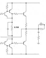
I had envisaged a double emitter follower with the first device, the driver, replaced by a CFP. The second device, the output transistor, is operating in simple common collector.
I prefer this arrangement because by the simple expedient of a resistor between the two emitters of the input devices we can keep the driver CFPs on all the time, avoiding the poor switch-off behaviour you referred to. There is still no compensation of the Vbe losses on the output devices, but these are dwarfed by the more linear compression conferred by the emitter resistors; with 0.15R emitter resistors, only 33% of the signal compression at peak is originated in the output devices (assuming 5200/1943).
It is becoming clear to me that in no other stage of an audio amplifier more compromised than in the output stage......
Thank you both!
Cheers,
Hugh
Mihai is correct - thank you Mihai! Pardon my not posting an image, I did not have one handy and time was, and remains, short!
I had envisaged a double emitter follower with the first device, the driver, replaced by a CFP. The second device, the output transistor, is operating in simple common collector.
I prefer this arrangement because by the simple expedient of a resistor between the two emitters of the input devices we can keep the driver CFPs on all the time, avoiding the poor switch-off behaviour you referred to. There is still no compensation of the Vbe losses on the output devices, but these are dwarfed by the more linear compression conferred by the emitter resistors; with 0.15R emitter resistors, only 33% of the signal compression at peak is originated in the output devices (assuming 5200/1943).
It is becoming clear to me that in no other stage of an audio amplifier more compromised than in the output stage......
Thank you both!
Cheers,
Hugh
AKSA said:Hi Edmond,
Mihai is correct - thank you Mihai! Pardon my not posting an image, I did not have one handy and time was, and remains, short!
I had envisaged a double emitter follower with the first device, the driver, replaced by a CFP. The second device, the output transistor, is operating in simple common collector.
I prefer this arrangement because by the simple expedient of a resistor between the two emitters of the input devices we can keep the driver CFPs on all the time, avoiding the poor switch-off behaviour you referred to. There is still no compensation of the Vbe losses on the output devices, but these are dwarfed by the more linear compression conferred by the emitter resistors; with 0.15R emitter resistors, only 33% of the signal compression at peak is originated in the output devices (assuming 5200/1943).
It is becoming clear to me that in no other stage of an audio amplifier more compromised than in the output stage......
Thank you both!
Cheers,
Hugh
Hello
Is it something like that ?
Thank
Bye
Gaetan
Attachments
Hello Hugh
Do that CFP driver output are easyer to drive for the VAS and can use a one transistor VAS ?
Thank
Bye
Gaétan
Do that CFP driver output are easyer to drive for the VAS and can use a one transistor VAS ?
Thank
Bye
Gaétan
Re: Re: Re: VAS
I agree, the CMCL is a good way to do a complementary symmetrical VAS. Our only difference, which I think is one largely of preference, is that I do not think a symmetrical VAS is necessary to achieve ultimate performance, even though it looks nice on the schematic.
A key issue for me is that I like to have a JFET input, and the poor availability/matching of complementary differential JFET pairs is a well-known problem. If one is OK with using BJTs in the input stage, then the full complementary input differential pair approach is a good choice.
The picture you refer to is barely a shadow of my favorite VAS; its main commonality is that it operates at 10 mA, has 10:1 degeneration, and is fed from a current mirror.
For those interested, a reasonable depiction and description of my favorite VAS is in my MOSFET amplifier paper under publications on my web site at www.cordellaudio.com.
Cheers,
Bob
Edmond Stuart said:
And that is precisely the reason why I'm so crazy about a common mode control loop (CMCL) of a symmetrical VAS, as this one does NOT spoil the VAS input by a resistor.
Cheers, Edmond.
PS: As for your favorite VAS, see my last picture. 😀

I agree, the CMCL is a good way to do a complementary symmetrical VAS. Our only difference, which I think is one largely of preference, is that I do not think a symmetrical VAS is necessary to achieve ultimate performance, even though it looks nice on the schematic.
A key issue for me is that I like to have a JFET input, and the poor availability/matching of complementary differential JFET pairs is a well-known problem. If one is OK with using BJTs in the input stage, then the full complementary input differential pair approach is a good choice.
The picture you refer to is barely a shadow of my favorite VAS; its main commonality is that it operates at 10 mA, has 10:1 degeneration, and is fed from a current mirror.
For those interested, a reasonable depiction and description of my favorite VAS is in my MOSFET amplifier paper under publications on my web site at www.cordellaudio.com.
Cheers,
Bob
AKSA said:Hi Edmond,
Mihai is correct - thank you Mihai! Pardon my not posting an image, I did not have one handy and time was, and remains, short!
I had envisaged a double emitter follower with the first device, the driver, replaced by a CFP. The second device, the output transistor, is operating in simple common collector.
I prefer this arrangement because by the simple expedient of a resistor between the two emitters of the input devices we can keep the driver CFPs on all the time, avoiding the poor switch-off behaviour you referred to. There is still no compensation of the Vbe losses on the output devices, but these are dwarfed by the more linear compression conferred by the emitter resistors; with 0.15R emitter resistors, only 33% of the signal compression at peak is originated in the output devices (assuming 5200/1943).
It is becoming clear to me that in no other stage of an audio amplifier more compromised than in the output stage......
Thank you both!
Cheers,
Hugh
I agree, Hugh. The output stage is the toughest challenge. I generally feel that crossover distortion in the output stage is the biggest culprit.
Cheers,
Bob
Re: Re: Re: Re: VAS
It not only looks nice on the schematic (ie a complementary symmetrical VAS), it does perform better:
1. Less noise, about 3dB.
2. Less input bias current.
3. More output current (from the VAS)
See, for example, our unbeatable PGP amp and also here:
http://www.diyaudio.com/forums/showthread.php?postid=1408551#post1408551
Besides, my latest symmetrical front-end comprises one tranny less than your front-end. It also contributes an unheard minuscule amount of distortion, 20ppb, to the THD at 20kHz.
Cheers, Edmond.
Bob Cordell said:I agree, the CMCL is a good way to do a complementary symmetrical VAS. Our only difference, which I think is one largely of preference, is that I do not think a symmetrical VAS is necessary to achieve ultimate performance, even though it looks nice on the schematic.
A key issue for me is that I like to have a JFET input, and the poor availability/matching of complementary differential JFET pairs is a well-known problem. If one is OK with using BJTs in the input stage, then the full complementary input differential pair approach is a good choice.
The picture you refer to is barely a shadow of my favorite VAS; its main commonality is that it operates at 10 mA, has 10:1 degeneration, and is fed from a current mirror.
For those interested, a reasonable depiction and description of my favorite VAS is in my MOSFET amplifier paper under publications on my web site at www.cordellaudio.com.
Cheers,
Bob
It not only looks nice on the schematic (ie a complementary symmetrical VAS), it does perform better:
1. Less noise, about 3dB.
2. Less input bias current.
3. More output current (from the VAS)
See, for example, our unbeatable PGP amp and also here:
http://www.diyaudio.com/forums/showthread.php?postid=1408551#post1408551
Besides, my latest symmetrical front-end comprises one tranny less than your front-end. It also contributes an unheard minuscule amount of distortion, 20ppb, to the THD at 20kHz.
Cheers, Edmond.
Bob Cordell said:
I agree, Hugh. The output stage is the toughest challenge. I generally feel that crossover distortion in the output stage is the biggest culprit.
Cheers,
Bob
That's new to me!

Re: Re: Re: Re: Re: VAS
1. not necessarily
2. certainly not when JFETs are used
3. Not at all
You may have one less transistor, but the complexity of the CMCL is at a whole 'nother level.
Cheers,
Bob
Edmond Stuart said:
It not only looks nice on the schematic (ie a complementary symmetrical VAS), it does perform better:
1. Less noise, about 3dB.
2. Less input bias current.
3. More output current (from the VAS)
See, for example, our unbeatable PGP amp and also here:
http://www.diyaudio.com/forums/showthread.php?postid=1408551#post1408551
Besides, my latest symmetrical front-end comprises one tranny less than your front-end. It also contributes an unheard minuscule amount of distortion, 20ppb, to the THD at 20kHz.
Cheers, Edmond.
1. not necessarily
2. certainly not when JFETs are used
3. Not at all
You may have one less transistor, but the complexity of the CMCL is at a whole 'nother level.
Cheers,
Bob
Re: Re: Re: Re: Re: Re: VAS
1. Doubling the number of input stages always reduces the noise by 3dB. (provided that Zo of the signal source is sufficiently low)
2. JFETs have (generally) a larger Vos. So what's the deal?
3. Not at all? What's the max. output current of your VAS?
the complexity of the CMCL ? four more trannies? RTFP!
edit: my latest symmetrical front-end comprises one tranny less than your front-end, including the trannies of the CMCL.
Bob Cordell said:1. not necessarily
2. certainly not when JFETs are used
3. Not at all
You may have one less transistor, but the complexity of the CMCL is at a whole 'nother level.
Cheers,
Bob
1. Doubling the number of input stages always reduces the noise by 3dB. (provided that Zo of the signal source is sufficiently low)
2. JFETs have (generally) a larger Vos. So what's the deal?
3. Not at all? What's the max. output current of your VAS?
the complexity of the CMCL ? four more trannies? RTFP!
edit: my latest symmetrical front-end comprises one tranny less than your front-end, including the trannies of the CMCL.
Re: Re: Re: Re: Re: Re: VAS
Hi Bob,
What do you mean by "Not at all"?
An ordinary VAS can deliver a max current of say 10mA
Your VAS 18mA
My VAS in the non-HEC amp 50mA
And in the PGP amp 100mA (deliberately limited to this value to protect the trannies from self destruction)
Cheers, Edmond.
Bob Cordell said:[snip]
3. Not at all
[snip]
Cheers,
Bob [/B]
Hi Bob,
What do you mean by "Not at all"?
An ordinary VAS can deliver a max current of say 10mA
Your VAS 18mA
My VAS in the non-HEC amp 50mA
And in the PGP amp 100mA (deliberately limited to this value to protect the trannies from self destruction)
Cheers, Edmond.
Re: Re: Re: Re: Re: Re: Re: VAS
WRT noise analysis, if you are referring to this design:
http://www.diyaudio.com/forums/attachment.php?s=&postid=1408551&stamp=1201094273
I think all is not as simple as first appears.
AFAICS, this constitutes a current FB architecture on the - IP as
such it has much higher current noise, maybe 10 ~ 15 pA/rtHz which
will react with FB R and R to ground.
http://focus.ti.com/lit/an/sboa066a/sboa066a.pdf
This and the value of IP R + FB R is likely to over ride the voltage
noise of the IP devices themselves unless a) they are extremely
noisy devices or b) extremely low value FB / IP R's are used.
WRT the Jfet dif pair IP design, assuming low noise Jfets (1nV/rt Hz),
again the source degen R's, IP R and FB R values will far over ride
the IP devices voltage noise.
Either way, the noise is not really an issue, both designs can be
very low noise. The noise on recordings from mics and mic
pres will be massively higher than what these amps will have.
I think we need to lighten up here a bit, we are not saving the world
- it's supposed to be enjoyable. 😎
T
Edmond Stuart said:
1. Doubling the number of input stages always reduces the noise by 3dB. (provided that Zo of the signal source is sufficiently low)
2. JFETs have (generally) a larger Vos. So what's the deal?
3. Not at all? What's the max. output current of your VAS?
the complexity of the CMCL ? four more trannies? RTFP!
edit: my latest symmetrical front-end comprises one tranny less than your front-end, including the trannies of the CMCL.
WRT noise analysis, if you are referring to this design:
http://www.diyaudio.com/forums/attachment.php?s=&postid=1408551&stamp=1201094273
I think all is not as simple as first appears.
AFAICS, this constitutes a current FB architecture on the - IP as
such it has much higher current noise, maybe 10 ~ 15 pA/rtHz which
will react with FB R and R to ground.
http://focus.ti.com/lit/an/sboa066a/sboa066a.pdf
This and the value of IP R + FB R is likely to over ride the voltage
noise of the IP devices themselves unless a) they are extremely
noisy devices or b) extremely low value FB / IP R's are used.
WRT the Jfet dif pair IP design, assuming low noise Jfets (1nV/rt Hz),
again the source degen R's, IP R and FB R values will far over ride
the IP devices voltage noise.
Either way, the noise is not really an issue, both designs can be
very low noise. The noise on recordings from mics and mic
pres will be massively higher than what these amps will have.
I think we need to lighten up here a bit, we are not saving the world
- it's supposed to be enjoyable. 😎
T
Re: Re: Re: Re: Re: Re: Re: Re: VAS
Hi Terry,
Actually, I was not referring to that design, rather amplifiers with a complementary VAS, which generally have two LPTs (one NPN and one PNP) in parallel, for example in our PGP amp.
It's a very old trick to reduce noise by paralleling multiple input stages. See John Curl's stuff, for example.
Although it's true that CFB input stage produce more current noise, it's not a real problem when source and NFB impedances are kept low. The noise from my CFB input stage is only about 50% more than from the PGP amp, mainly because of higher NFB resistors.
Cheers, Edmond.
PS: You didn't answer my question yet.
Terry Demol said:
WRT noise analysis, if you are referring to this design:
http://www.diyaudio.com/forums/attachment.php?s=&postid=1408551&stamp=1201094273
I think all is not as simple as first appears.
AFAICS, this constitutes a current FB architecture on the - IP as
such it has much higher current noise, maybe 10 ~ 15 pA/rtHz which
will react with FB R and R to ground.
[snip]
T
Hi Terry,
Actually, I was not referring to that design, rather amplifiers with a complementary VAS, which generally have two LPTs (one NPN and one PNP) in parallel, for example in our PGP amp.
It's a very old trick to reduce noise by paralleling multiple input stages. See John Curl's stuff, for example.
Although it's true that CFB input stage produce more current noise, it's not a real problem when source and NFB impedances are kept low. The noise from my CFB input stage is only about 50% more than from the PGP amp, mainly because of higher NFB resistors.
Cheers, Edmond.
PS: You didn't answer my question yet.
Re: Re: Re: Re: Re: Re: Re: VAS
Hi Edmond,
1. That is an incorrect generalization. It is often true if one doubles the number of identical input stages AND if noise is dominated by the noise of the input stage. However, a single input stage has equally low noise, all else remaining equal, if its operating currents are doubled and noise is not dominated by RB.
In reality, in most power amplifiers, the total effective source resistance is not so low as to not dominate or have a strong influence. Even if the signal source impedance is zero, there is the impedance of the feedback network. A 1k feedback network impedance will, for example, alone generate about 4 nV/rt Hz.
Going too low on the feedback network impedance can cause low-frequency nonlinearity issues in the feedback resistor as a result of temperature fluctuations with signal as a result of power dissipation (I always recommend using at least a 2 Watt feedback resistor).
The emitter degeneration resistors in the input stage also contribute noise. In general, the voltage noise contributed by a resistor is on the order of 0.13 nV/rt Hz per rt Ohm.
My amplifiers, using my input/VAS with a JFET input pair usually come in at around 5-7 nV/rt Hz. Note that a 5 nV/rt Hz input noise in an unwieghted 20 khz bandwidth yields an S/N with respect to 1 V rms input of 120 dB. This is quite a bit better than most amplifiers out there by a good deal. Anything lower than this is gravy.
2. JFETs have larger Vos, but you were asking about input current. A few mV of input offset is taken care of by any decent servo bias controller. Also bear in mind that input noise current can be an issue for bipolars much more than for JFETs.
3. The maximum output current of just about any VAS will be double the standing current of the VAS, as long as you are not foolish enough to venture into Class-AB VAS operation. My VAS, with 10 mA standing current, is capable of about 20 mA maximum output current, which is plenty when one is driving an output Triple or otherwise well-buffered output stage.
Complexity of a circuit is not just measured in the number of transistors. The conceptual complexity of your circuit is high in that it introduces another clever feedback loop, which more than one smart person on this board did not grasp immediately. What about the stability of this added loop? What does this loop do when the amplifier clips? The need to answer these questions suggests a higher level of conceptual complexity. Nevertheless, your circuit is a clever solution to an old problem that full complementary input/VAS architectures suffer from.
Cheers,
Bob
Edmond Stuart said:
1. Doubling the number of input stages always reduces the noise by 3dB. (provided that Zo of the signal source is sufficiently low)
2. JFETs have (generally) a larger Vos. So what's the deal?
3. Not at all? What's the max. output current of your VAS?
the complexity of the CMCL ? four more trannies? RTFP!
edit: my latest symmetrical front-end comprises one tranny less than your front-end, including the trannies of the CMCL.
Hi Edmond,
1. That is an incorrect generalization. It is often true if one doubles the number of identical input stages AND if noise is dominated by the noise of the input stage. However, a single input stage has equally low noise, all else remaining equal, if its operating currents are doubled and noise is not dominated by RB.
In reality, in most power amplifiers, the total effective source resistance is not so low as to not dominate or have a strong influence. Even if the signal source impedance is zero, there is the impedance of the feedback network. A 1k feedback network impedance will, for example, alone generate about 4 nV/rt Hz.
Going too low on the feedback network impedance can cause low-frequency nonlinearity issues in the feedback resistor as a result of temperature fluctuations with signal as a result of power dissipation (I always recommend using at least a 2 Watt feedback resistor).
The emitter degeneration resistors in the input stage also contribute noise. In general, the voltage noise contributed by a resistor is on the order of 0.13 nV/rt Hz per rt Ohm.
My amplifiers, using my input/VAS with a JFET input pair usually come in at around 5-7 nV/rt Hz. Note that a 5 nV/rt Hz input noise in an unwieghted 20 khz bandwidth yields an S/N with respect to 1 V rms input of 120 dB. This is quite a bit better than most amplifiers out there by a good deal. Anything lower than this is gravy.
2. JFETs have larger Vos, but you were asking about input current. A few mV of input offset is taken care of by any decent servo bias controller. Also bear in mind that input noise current can be an issue for bipolars much more than for JFETs.
3. The maximum output current of just about any VAS will be double the standing current of the VAS, as long as you are not foolish enough to venture into Class-AB VAS operation. My VAS, with 10 mA standing current, is capable of about 20 mA maximum output current, which is plenty when one is driving an output Triple or otherwise well-buffered output stage.
Complexity of a circuit is not just measured in the number of transistors. The conceptual complexity of your circuit is high in that it introduces another clever feedback loop, which more than one smart person on this board did not grasp immediately. What about the stability of this added loop? What does this loop do when the amplifier clips? The need to answer these questions suggests a higher level of conceptual complexity. Nevertheless, your circuit is a clever solution to an old problem that full complementary input/VAS architectures suffer from.
Cheers,
Bob
Re: VAS
Hi Bob,
I agree with most of your points. In the past you asked me the same question (about the benefits of a symmetrical front end), so you know already that our theoretical views don't differ at all.
It's because of some practical implications that I prefer a fully symmetrical topology, for example: one cannot always simply double the current, without exceeding the max. (or preferred) power dissipation of the input transistors.
As for the maximum output current of the VAS, mine easily exceeds two times the standing current without entering class B. The 'other' VAS is never turned off completely.
As for the common mode control loop, of course one have to pay attention to the stability of the CMCL (ie loop gain and phase margin). To get it right, however, is far from complex. in fact, the easiest task wrt all other pitfalls. If you look at my non-HEC amp for example,
http://www.diyaudio.com/forums/attachment.php?s=&postid=1367089&stamp=1196786670
a stable loop is 'automatically' achieved by means of the DTMC caps C4 and C5. Aren't you splitting hairs?
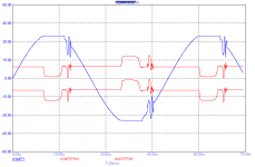
As for clipping, with or without CMCL, it doesn't matter as in both cases additional circuitry is necessary to ensure a decent behavior at overdrive conditions. I have also added such circuitry (not published yet) to the non-HEC amp and it performs quite well, I should say. See picture below. Also notice that the VAS currents are unaffected. Have you seen this ever before? I guess not.
Cheers, Edmond.
Bob Cordell said:Hi Edmond,
1. That is an incorrect generalization. It is often true if one doubles the number of identical input stages AND if noise is dominated by the noise of the input stage. However, a single input stage has equally low noise, all else remaining equal, if its operating currents are doubled and noise is not dominated by RB.
In reality, in most power amplifiers, the total effective source resistance is not so low as to not dominate or have a strong influence. Even if the signal source impedance is zero, there is the impedance of the feedback network. A 1k feedback network impedance will, for example, alone generate about 4 nV/rt Hz.
Going too low on the feedback network impedance can cause low-frequency nonlinearity issues in the feedback resistor as a result of temperature fluctuations with signal as a result of power dissipation (I always recommend using at least a 2 Watt feedback resistor).
The emitter degeneration resistors in the input stage also contribute noise. In general, the voltage noise contributed by a resistor is on the order of 0.13 nV/rt Hz per rt Ohm.
My amplifiers, using my input/VAS with a JFET input pair usually come in at around 5-7 nV/rt Hz. Note that a 5 nV/rt Hz input noise in an unwieghted 20 khz bandwidth yields an S/N with respect to 1 V rms input of 120 dB. This is quite a bit better than most amplifiers out there by a good deal. Anything lower than this is gravy.
2. JFETs have larger Vos, but you were asking about input current. A few mV of input offset is taken care of by any decent servo bias controller. Also bear in mind that input noise current can be an issue for bipolars much more than for JFETs.
3. The maximum output current of just about any VAS will be double the standing current of the VAS, as long as you are not foolish enough to venture into Class-AB VAS operation. My VAS, with 10 mA standing current, is capable of about 20 mA maximum output current, which is plenty when one is driving an output Triple or otherwise well-buffered output stage.
Complexity of a circuit is not just measured in the number of transistors. The conceptual complexity of your circuit is high in that it introduces another clever feedback loop, which more than one smart person on this board did not grasp immediately. What about the stability of this added loop? What does this loop do when the amplifier clips? The need to answer these questions suggests a higher level of conceptual complexity. Nevertheless, your circuit is a clever solution to an old problem that full complementary input/VAS architectures suffer from.
Cheers,
Bob
Hi Bob,
I agree with most of your points. In the past you asked me the same question (about the benefits of a symmetrical front end), so you know already that our theoretical views don't differ at all.
It's because of some practical implications that I prefer a fully symmetrical topology, for example: one cannot always simply double the current, without exceeding the max. (or preferred) power dissipation of the input transistors.
As for the maximum output current of the VAS, mine easily exceeds two times the standing current without entering class B. The 'other' VAS is never turned off completely.
As for the common mode control loop, of course one have to pay attention to the stability of the CMCL (ie loop gain and phase margin). To get it right, however, is far from complex. in fact, the easiest task wrt all other pitfalls. If you look at my non-HEC amp for example,
http://www.diyaudio.com/forums/attachment.php?s=&postid=1367089&stamp=1196786670
a stable loop is 'automatically' achieved by means of the DTMC caps C4 and C5. Aren't you splitting hairs?
As for clipping, with or without CMCL, it doesn't matter as in both cases additional circuitry is necessary to ensure a decent behavior at overdrive conditions. I have also added such circuitry (not published yet) to the non-HEC amp and it performs quite well, I should say. See picture below. Also notice that the VAS currents are unaffected. Have you seen this ever before? I guess not.
Cheers, Edmond.
Attachments
Re: Re: VAS
Hi Edmond,
In cases where a cascode is used, doubling of the current would not matter a lot in regard to power dissipation in the input stage. For example, I often bias my input FET pair with a tail current of 2-4 mA. Doubling this to 4-8 mA with a cascode at about +15V will only result in a max total dissipation in the FET pair of about 120 mW.
I must be missing something about your circuit's maximum VAS output current, or perhaps we are defining Class-A operation of the VAS differently. If you have a VAS standing current of 10 mA, and you can swing it to well beyond 20 mA, and the other VAS transistor does not shut off, I'm not sure I would call that Class-A. For one thing, it seems that such operation would imply an increase in the instantaneous common-mode current.
My definition of Class A may be different than yours. One side not turning off is necessary, but not sufficient for Class A, in my opinion. My view of Class-A is that both transistors are contributing about the same amount of transconductance to the output over the full swing. I don't see how that can be the case if one transistor well exceeds twice the standing current in signal swing.
Am I missing something here, or do we just disagree on the definition of Class-A?
Thanks,
Bob
Edmond Stuart said:
Hi Bob,
I agree with most of your points. In the past you asked me the same question (about the benefits of a symmetrical front end), so you know already that our theoretical views don't differ at all.
It's because of some practical implications that I prefer a fully symmetrical topology, for example: one cannot always simply double the current, without exceeding the max. (or preferred) power dissipation of the input transistors.
As for the maximum output current of the VAS, mine easily exceeds two times the standing current without entering class B. The 'other' VAS is never turned off completely.
Cheers, Edmond.
Hi Edmond,
In cases where a cascode is used, doubling of the current would not matter a lot in regard to power dissipation in the input stage. For example, I often bias my input FET pair with a tail current of 2-4 mA. Doubling this to 4-8 mA with a cascode at about +15V will only result in a max total dissipation in the FET pair of about 120 mW.
I must be missing something about your circuit's maximum VAS output current, or perhaps we are defining Class-A operation of the VAS differently. If you have a VAS standing current of 10 mA, and you can swing it to well beyond 20 mA, and the other VAS transistor does not shut off, I'm not sure I would call that Class-A. For one thing, it seems that such operation would imply an increase in the instantaneous common-mode current.
My definition of Class A may be different than yours. One side not turning off is necessary, but not sufficient for Class A, in my opinion. My view of Class-A is that both transistors are contributing about the same amount of transconductance to the output over the full swing. I don't see how that can be the case if one transistor well exceeds twice the standing current in signal swing.
Am I missing something here, or do we just disagree on the definition of Class-A?
Thanks,
Bob
Re: Clipping
Wow, that's pretty ugly! Is that how the CMCL VAS behaves in clipping if special clipping measures are not taken?
A more conventional input/VAS circuit, even without clipping measures like Baker clamps, does not behave that badly.
Cheers,
Bob
Edmond Stuart said:And here is an example of what might happen if less attention is paid to the clipping behavior.
Wow, that's pretty ugly! Is that how the CMCL VAS behaves in clipping if special clipping measures are not taken?
A more conventional input/VAS circuit, even without clipping measures like Baker clamps, does not behave that badly.
Cheers,
Bob
Re: Re: Re: VAS
Hi Bob,
Indeed, you are missing something. For example. the patience and the willing to read my post more carefully.
I'm not redefining the meaning of class-A, I haven't even used that term.
I only said that "The 'other' VAS is never turned off completely.", and I really don't care how well it fits into some type of class.
Cheers, Edmond.
Bob Cordell said:Hi Edmond,
[snip]
I must be missing something about your circuit's maximum VAS output current, or perhaps we are defining Class-A operation of the VAS differently. If you have a VAS standing current of 10 mA, and you can swing it to well beyond 20 mA, and the other VAS transistor does not shut off, I'm not sure I would call that Class-A. For one thing, it seems that such operation would imply an increase in the instantaneous common-mode current.
My definition of Class A may be different than yours. One side not turning off is necessary, but not sufficient for Class A, in my opinion. My view of Class-A is that both transistors are contributing about the same amount of transconductance to the output over the full swing. I don't see how that can be the case if one transistor well exceeds twice the standing current in signal swing.
Am I missing something here, or do we just disagree on the definition of Class-A?
Thanks,
Bob
Hi Bob,
Indeed, you are missing something. For example. the patience and the willing to read my post more carefully.
I'm not redefining the meaning of class-A, I haven't even used that term.
I only said that "The 'other' VAS is never turned off completely.", and I really don't care how well it fits into some type of class.
Cheers, Edmond.
- Home
- Amplifiers
- Solid State
- Bob Cordell Interview: Error Correction