Elektor Electronics have agreed that I can post the schematics of my ec power amp on-line. The first article appeared in the April issue and described the output power stage. Circuit below.
Part 2 (Vas) and part 3 (comprehensive protection system) will appear in the May issue. I will post schematics when they are available.
Feedback, global or not 😉 is welcome!
Jan Didden
Part 2 (Vas) and part 3 (comprehensive protection system) will appear in the May issue. I will post schematics when they are available.
Feedback, global or not 😉 is welcome!
Jan Didden
Attachments
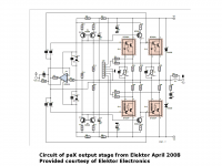
janneman said:Elektor Electronics have agreed that I can post the schematics of my ec power amp on-line. The first article appeared in the April issue and described the output power stage. Circuit below.
Part 2 (Vas) and part 3 (comprehensive protection system) will appear in the May issue. I will post schematics when they are available.
Feedback, global or not 😉 is welcome!
Jan Didden
Jan,
Can you give us some brief performance specifications. Power,
distortion at max power / 20kHz / 4ohm / 8 ohm etc.
What was the design intent?
Thanks,
Terry
Terry Demol said:
Jan,
Can you give us some brief performance specifications. Power,
distortion at max power / 20kHz / 4ohm / 8 ohm etc.
What was the design intent?
Thanks,
Terry
Hi Terry,
Design intent was twofold: see what you can get with only ec (the Vas has it's own ec loop) without a gnfb loop; and get rid of thermal (memory?) distortion. I don't know if I got to the last goal as I haven't done any measurements on that yet. Long-term thermal stability is OK but I was interested in avoiding shift of bias point after high-power bursts. So I still need to verify how that is.
Power is 100/8, 200/4. I have a few graphs in part 2, lets say THD is about 0.005% at lower freqs, rising to 0.05% at 20kHz, until just before clipping.
I think the way it works is not really obvious from the schematic; probably worthwhile to download the English version of the article from the Elektor UK website:
http://www.elektor.com/magazines/20...ier-with-error-correction-part-1.399028.lynkx
Cost is about $ 1.80 I think. As author I have a some 'Elektor credits' to download a few copies but obviously I can't post the article here.
Edit: You can pay the download with Paypal.
Jan Didden
janneman said:
Hi Terry,
Design intent was twofold: see what you can get with only ec (the Vas has it's own ec loop) without a gnfb loop; and get rid of thermal (memory?) distortion. I don't know if I got to the last goal as I haven't done any measurements on that yet. Long-term thermal stability is OK but I was interested in avoiding shift of bias point after high-power bursts. So I still need to verify how that is.
Yes thermal related effects are a problem and those Sanken devices
should solve it. I thought of using them myself, the only bug is you
don't get to control current through first BJT of the darlington pair.
Power is 100/8, 200/4. I have a few graphs in part 2, lets say THD is about 0.005% at lower freqs, rising to 0.05% at 20kHz, until just before clipping.
OK so it's not quite a PGP but certainly very good performance for a
sans global FB design.
I think the way it works is not really obvious from the schematic; probably worthwhile to download the English version of the article from the Elektor UK website:
I understand it and think it is very clever. Particularly the way you
have utilised the open loop connection of 844 to be a) an I-V b)
EC 'comparator' and c) driver for OP devices all in one hit.
http://www.elektor.com/magazines/20...ier-with-error-correction-part-1.399028.lynkx
Cost is about $ 1.80 I think. As author I have a some 'Elektor credits' to download a few copies but obviously I can't post the article here.
Edit: You can pay the download with Paypal.
Jan Didden
Thanks I'll check it out.
Terry Demol said:Yes thermal related effects are a problem and those Sanken devices should solve it. I thought of using them myself, the only bug is you don't get to control current through first BJT of the darlington pair.[snip
Yes indeed. Doesn't seem to harm too much though.
Terry Demol said:[snip]I understand it and think it is very clever. Particularly the way you have utilised the open loop connection of 844 to be a) an I-V b) EC 'comparator' and c) driver for OP devices all in one hit.
Thanks I'll check it out.
You got it....
Jan Didden
janneman said:
Yes indeed. Doesn't seem to harm too much though.
You got it....
Jan Didden
Hi Jan, nice piece of work.
How would you compare this implementation of HEC with the discrete transistor version that Hawksford and I used?
It will be very interesting to see how well the Sanken parts correct for the thermal stability following a power burst. I have curves showing that effect for a conventional BJT output stage (and MOSFET) in my original MOSFET error correction paper. I have always felt that that effect was a significant concern, especially with BJTs, as they can easily be left under-biased after a power burst. BTW, my work on that thermal problem predates that of the French guy you cited 🙂, although I would not be surprized if there is other work on this subject that predates mine.
What level of bias current flows through the Darlinton transistors in those Sanken parts? What is the rated ft of the Sanken parts?
Did you consider using OnSemi ThermalTrak devices as opposed to the Sankens?
Thanks,
Bob
Bob Cordell said:[snip]How would you compare this implementation of HEC with the discrete transistor version that Hawksford and I used?
[snip]
Hi Bob,
I'm not sure the two topologies can be directly compared because I also use H.ec in the Vas and no global nfb. The Vas ol gain is 20. With the ec loops the total amplifier performance is roughly comparable with a good 'traditional' amp. Of course, in your and other amps that use *both* output stage ec *and* global nfb (with a high ol gain) you can get better figures.
Anyway, my output stage with ec is not the limiting factor in the whole amp; the Vas and output stage have roughly the same linearity and the amp as whole also, the limiting factor is my particular ec implementation with the AD844 as CCII. It would be interesting to see what level can be reached with a better, possibly discrete, CCII implementation.
Bob Cordell said:[snip]It will be very interesting to see how well the Sanken parts correct for the thermal stability following a power burst. I have curves showing that effect for a conventional BJT output stage (and MOSFET) in my original MOSFET error correction paper. I have always felt that that effect was a significant concern, especially with BJTs, as they can easily be left under-biased after a power burst. BTW, my work on that thermal problem predates that of the French guy you cited 🙂, although I would not be surprized if there is other work on this subject that predates mine.
What level of bias current flows through the Darlinton transistors in those Sanken parts? What is the rated ft of the Sanken parts?
Did you consider using OnSemi ThermalTrak devices as opposed to the Sankens?
Thanks,
Bob
I did consider the OnSemi's but they are, in my view, just a 'me too' implementation of the Sanken idea; the OnSemi's don't have the carefully matched tempco between the diodes and the transistors. You have the diode on the die but you still need to tailor the bias circuit to make the tempco's track. Sanken did a great job there, and the effort can be seen in the fact that they used a single diode in the N-device and a string of 5 schottky's in the P device. The result is pretty good tracking, IF you use 2.5mA through the diodes and 40mA quiescent current. I did cheat though, because 40mA is just at the border wrt xover distortion. I run mine at 55mA, still good enough (long term) temp tracking and very little xover.
Sanken is very sparse with the specs; Ft isn't specified. The Hfe vs Ic is nicely linear (on a log scale: 1000 typ at .1A, 10,000 at 10A. Kind of inverse beta droop.
Funny thing with those Sankens: the original versions labelled SAP16N, P had also the Re (0.22 ohms) on the die for even less pcb real estate. But they found out that those Re's had a smaller SOA than the darlingtons themselves; the Re's blew before the transistors, and that of course made you replace the whole thing.
The versions labelled STD03N, P don't have the Re, and that pin is still sticking out but cut off. If they only had brought out the driver emitter out to that pin!
Anybody here who has some clout with Sanken??
Jan Didden
Hi, Janneman,
Nice CCT 😀
Nice CCT 😀
Why it needs an I-V? It won't work with voltage opamp?to be a) an I-V
lumanauw said:Hi, Janneman,
Nice CCT 😀
Why it needs an I-V? It won't work with voltage opamp?
Hi David,
Yes it will work also with a regular opamp. I just didn't want to use a high-feedback opamp stage as a summer in an ec power amp. No real engineering reasons for it, I'm afraid 😉 .
Jan Didden
Hi Jan,
very clever design you did, this boostrapping / current "stealing" hookup. But why did you(?) choose to draw the schematic in this obscure way (opamp reversed, all those paralled R//C loitering around) 😀
IMHO this is a perfect example that e.c. == loop feedback, at times. To me it looks like a nicely designed but otherwise "ordinary" full feedback power buffer. In the end it's only a point-of-view issue how you name it, d'accord?
Nevertheless, let's argue a little. E.c. I would understand as a mechanism which might be null-trimmed, the pos/neg feedback balancing that was discussed here to big extend. Somehow something *on top* of an existing forward path (one might regard this forward path the one we would have if the opamp were running as a local buffer with its loop closed locally instead of globally around the output. And the null-trimming is "automatic").
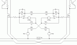
To better illustrate what I mean look at the attached circuit, the stripped core of a e.c. circlotron I'm fiddling with (cascoded, D2S-biased and xformer coupled, btw). Without R4 in place we would have a simple source follower config (with gain 1+R2/R1). It would have a finite Zout of 1/(2*gm) and any change in the gm would introduce distortion, in this case, when leaving the constant gm D2S portion, it would be expanding odd order slope distortion.
When R4 is set such that R1/R2=R3/R4 we get full cancelling of distortion and zero output impedance (to the amount loop gain allows us to reach that ideal), further signal gain is doubled in value. If R4 is larger, cancelling isn't perfect and Zout is slightly positive. If R4 is lower than optimum, cancelling again isn't perfect (and opposite in effect, error residue swaps in polarity) and the output impedance gets negative. This would be the the pos fb > neg fb case. In your circuit, this case cannot happen. Which surely does no harm to its peformance, and I definitly don't want to reopen the e.c. vs nfb sematics battle that we have seen in this thread.
- Klaus
very clever design you did, this boostrapping / current "stealing" hookup. But why did you(?) choose to draw the schematic in this obscure way (opamp reversed, all those paralled R//C loitering around) 😀
IMHO this is a perfect example that e.c. == loop feedback, at times. To me it looks like a nicely designed but otherwise "ordinary" full feedback power buffer. In the end it's only a point-of-view issue how you name it, d'accord?
Nevertheless, let's argue a little. E.c. I would understand as a mechanism which might be null-trimmed, the pos/neg feedback balancing that was discussed here to big extend. Somehow something *on top* of an existing forward path (one might regard this forward path the one we would have if the opamp were running as a local buffer with its loop closed locally instead of globally around the output. And the null-trimming is "automatic").
To better illustrate what I mean look at the attached circuit, the stripped core of a e.c. circlotron I'm fiddling with (cascoded, D2S-biased and xformer coupled, btw). Without R4 in place we would have a simple source follower config (with gain 1+R2/R1). It would have a finite Zout of 1/(2*gm) and any change in the gm would introduce distortion, in this case, when leaving the constant gm D2S portion, it would be expanding odd order slope distortion.
When R4 is set such that R1/R2=R3/R4 we get full cancelling of distortion and zero output impedance (to the amount loop gain allows us to reach that ideal), further signal gain is doubled in value. If R4 is larger, cancelling isn't perfect and Zout is slightly positive. If R4 is lower than optimum, cancelling again isn't perfect (and opposite in effect, error residue swaps in polarity) and the output impedance gets negative. This would be the the pos fb > neg fb case. In your circuit, this case cannot happen. Which surely does no harm to its peformance, and I definitly don't want to reopen the e.c. vs nfb sematics battle that we have seen in this thread.
- Klaus
Attachments
Jan,
now I get it (the summing action w/o feedback)... the use of AD844's TZ pin seems to do the trick. I stand corrected, NO full loop feedback. Great!
- Klaus
now I get it (the summing action w/o feedback)... the use of AD844's TZ pin seems to do the trick. I stand corrected, NO full loop feedback. Great!
- Klaus
KSTR said:[snip]To better illustrate what I mean look at the attached circuit, the stripped core of a e.c. circlotron I'm fiddling with (cascoded, D2S-biased and xformer coupled, btw). Without R4 in place we would have a simple source follower config (with gain 1+R2/R1). It would have a finite Zout of 1/(2*gm) and any change in the gm would introduce distortion, in this case, when leaving the constant gm D2S portion, it would be expanding odd order slope distortion.
When R4 is set such that R1/R2=R3/R4 we get full cancelling of distortion and zero output impedance (to the amount loop gain allows us to reach that ideal), further signal gain is doubled in value. If R4 is larger, cancelling isn't perfect and Zout is slightly positive. If R4 is lower than optimum, cancelling again isn't perfect (and opposite in effect, error residue swaps in polarity) and the output impedance gets negative. This would be the the pos fb > neg fb case. In your circuit, this case cannot happen. Which surely does no harm to its peformance, and I definitly don't want to reopen the e.c. vs nfb sematics battle that we have seen in this thread.- Klaus
Hmm, you're going a bit too fast for me now, I need to digest it.
KSTR said:Hi Jan,
very clever design you did, this boostrapping / current "stealing" hookup. But why did you(?) choose to draw the schematic in this obscure way (opamp reversed, all those paralled R//C loitering around) 😀
[snip]- Klaus
Yes, it does look funny, doesn't it? I have at least three different ways of drawing this that I tried out, without being happy with it. Anytime you draw it the 'conventional way - pointing to the right - your mind automatically says: "aha, opamp", which of course it isn't. The input to the circuit is at pin 5, NOT pin 3 (or 2). So I decided to draw it a bit lopsided to avoid the automatic "aha, opamp" and force people to think a bit.
Jan Didden
KSTR said:Jan,
now I get it (the summing action w/o feedback)... the use of AD844's TZ pin seems to do the trick. I stand corrected, NO full loop feedback. Great!
- Klaus
... obviously my ploy worked, no 😉 ?
Jan Didden
Very interesting implementation - I wandered off to look at the circuit and other material linked from your web site before I read the replies (IIRC I fell into this thread by way of a reference to PaX, and I've spent far too much time reading the backstory of this thread... and sitting on my hands a lot so as not to clutter it with probably duplicate replies to years-old discussions).
I'd swear I've seen some specialized parts with on-chip diodes for thermally compensated bias long ago - RF parts, maybe? Anyway, I'm less impressed with the Sanken parts. Oh, they're clever in some respects, but when I look at the assymetrical sensing diodes and the pinout, it tends to suggest to me an overspecialized design. The paranoid part of me thinks about what an excellent design lock-in feature that is...
The thermal tracking relies on both devices being mounted on the same heatsink, don't you think? It's so assymetrical that it can only track well if both devices are at the same temperature. I'm not sure how well that will work out for low frequency thermal compensation even on the same heatsink...
The OnSemi NJL parts are indeed less engineered for a simple, specific circuit, but I tend to think of that as "less specialized", and don't see it as an inherent drawback. Certainly the Sanken parts are simpler to apply if you need only a single pair and care more about simplifying a moderate-performing circuit than achieving a more interesting level of performance (doesn't that bias requirement fairly scream "just hook us between the VAS collectors, that will work well enough"?). Without meaning to in any way denigrate your impressive achievement there, I do think the clutter of the circuitry needed to drive the Sankens in the manner their biasing requires argues that point better than I can.
janneman said:
I did consider the OnSemi's but they are, in my view, just a 'me too' implementation of the Sanken idea; the OnSemi's don't have the carefully matched tempco between the diodes and the transistors. You have the diode on the die but you still need to tailor the bias circuit to make the tempco's track.
I'd swear I've seen some specialized parts with on-chip diodes for thermally compensated bias long ago - RF parts, maybe? Anyway, I'm less impressed with the Sanken parts. Oh, they're clever in some respects, but when I look at the assymetrical sensing diodes and the pinout, it tends to suggest to me an overspecialized design. The paranoid part of me thinks about what an excellent design lock-in feature that is...
The thermal tracking relies on both devices being mounted on the same heatsink, don't you think? It's so assymetrical that it can only track well if both devices are at the same temperature. I'm not sure how well that will work out for low frequency thermal compensation even on the same heatsink...
The OnSemi NJL parts are indeed less engineered for a simple, specific circuit, but I tend to think of that as "less specialized", and don't see it as an inherent drawback. Certainly the Sanken parts are simpler to apply if you need only a single pair and care more about simplifying a moderate-performing circuit than achieving a more interesting level of performance (doesn't that bias requirement fairly scream "just hook us between the VAS collectors, that will work well enough"?). Without meaning to in any way denigrate your impressive achievement there, I do think the clutter of the circuitry needed to drive the Sankens in the manner their biasing requires argues that point better than I can.
HEC implementation
One thought I had while reading older posts was about a variation on the HEC circuit which I played with in simulations. Like others, I've been a bit unhappy about having to develop even more "excess" voltage at the VAS output, though since I was working with MOS outputs I already needed more of that than a typical BJT design anyway. So one day I was frowning at that when it occurred to me that a voltage source through a resistance is equivalent to a current source shunted by a resistance...
Those sims appear to have been part of the Great WINE Meltdown, as I can't find them in the current working directories, so I'm not sure how exactly I had arranged it. I'd guess it was the first half of a "diamond follower", with resistors of a Kohm or two and 5-10 mA current sources. I probably need to find or recreate this...
Well it did, after a short delay...janneman said:The input to the circuit is at pin 5, NOT pin 3 (or 2). So I decided to draw it a bit lopsided to avoid the automatic "aha, opamp" and force people to think a bit.
[...]
obviously my ploy worked, no 😉 ?
A thoughtful decision of yours, just because of this "aha, opamp" gotcha I myself trapped into when looking the circuit for the first time -- looking closer was required. It seems that what I first took the circuit for, a full nfb loop with a conventional opamp hookup -- the unity gain, in-the-loop power puffer approach --, would work also (set aside the stabilty problems) but that is just what your idea wanted to circumvent, right?
Maybe the use of a non-opamp circuit symbol would have done the trick even better ... the next time you publish this trick 🙂
- Klaus
Regarding the temporal bias drift under changing load conditions, has anyone ever thought about a servo style circuit which measures the actual bias current and adjusts it? With the cascoded circlotron approach it is quite easy to track the sum of the transistor currents without the use of degeneration/current sensing resistors in the main pair, and the minimum of it (occuring during output current zero crossings), which is the actual bias, could be captured with a peak detector (with droop, of course), smoothed, processed and summed into the thermally derived bias. Which would be especially useful if the thermal loop tracking and time constant is large and unreliable, when using devices without on-die temp sensing means but a traditional heatsink-mounted Vbe-mult instead.
- Klaus
- Klaus
autobias of mosfets
Hi Klaus,
Yes, I did exactly that. Look here: http://home.tiscali.nl/data.odyssey/AutoBias.html
Cheers, Edmond.
KSTR said:Regarding the temporal bias drift under changing load conditions, has anyone ever thought about a servo style circuit which measures the actual bias current and adjusts it? With the cascoded circlotron approach it is quite easy to track the sum of the transistor currents without the use of degeneration/current sensing resistors in the main pair, and the minimum of it (occuring during output current zero crossings), which is the actual bias, could be captured with a peak detector (with droop, of course), smoothed, processed and summed into the thermally derived bias. Which would be especially useful if the thermal loop tracking and time constant is large and unreliable, when using devices without on-die temp sensing means but a traditional heatsink-mounted Vbe-mult instead.
- Klaus
Hi Klaus,
Yes, I did exactly that. Look here: http://home.tiscali.nl/data.odyssey/AutoBias.html
Cheers, Edmond.
Another great circuit idea of you, Edmond. Have to digest it slowly, I guess.
In fact this circuit looks quite close to what I have in mind, one difference being that I wanted to use the true minimum instead of average of the output current (which is more or less identical only while in class-A), compare that to a reference, feeding a servo in turn. I feel that sensing the minimum might be essential to keep things in order, under large class B operation. It's intended for a D2S stage where, when used without e.c./feedback, keeping the correct bias will be essential (and this optimum might still be itself dependent on actual die temp, something I would need to investigate). There still is the problem then wether the minimum detector is fast enough to catch the sometimes very quick transition through the minimum, same problem that you see, I read. That's why I think of having regular "slow" temp sensing and only adjust its op point with the quicker servo over a limited range.
- Klaus
- Home
- Amplifiers
- Solid State
- Bob Cordell Interview: Error Correction