Continuing from here.
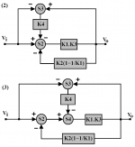
To better visualize how a ''desensitizer'' with gain might be implemented, the block-diagrams here are further manipulated in an elementary step that generates new summer S4 below, which shows that this loop need not be associated with summing point S2.
This, i suspect, makes life slightly easier....(?)
Note that the transfer function derived here remains correct.
Attachments
Experimentation reveals that this arrangement appears surprisingly insensitive to modest (~10%) imbalances in the error amplifiers.
This probably because the complementary error amps. tend to cancel such errors; this also appears to be attribute of Hawksford's scheme.
This probably because the complementary error amps. tend to cancel such errors; this also appears to be attribute of Hawksford's scheme.
Re: Re: Re: Re: Controlled clipping of EC amplifiers
Heinz wrote:
Then, less than an hour later, Heinz posted:
Heinz, once again thank you very much! This is exactly what I was looking for. It appears to have very high attenuation of the ripple from the unregulated supply, yet responds very fast to reductions in the unregulated supply voltage. And it is not at all complex either. Very clever. It shows the superiority of a nonlinear "min hold" approach to that of simple low-pass filtering. I will definitely incorporate a minor variation of this into my project. Thanks again.
I'm signing off until shortly after the new year due to being on travel to visit family for the holidays. Happy holidays and happy new year!
Heinz wrote:
powerbecker said:I have to think, if there is a more direct way to do the same at high voltages. Currently I have no idea!
Then, less than an hour later, Heinz posted:
powerbecker said:Possibly this?
Heinz, once again thank you very much! This is exactly what I was looking for. It appears to have very high attenuation of the ripple from the unregulated supply, yet responds very fast to reductions in the unregulated supply voltage. And it is not at all complex either. Very clever. It shows the superiority of a nonlinear "min hold" approach to that of simple low-pass filtering. I will definitely incorporate a minor variation of this into my project. Thanks again.
I'm signing off until shortly after the new year due to being on travel to visit family for the holidays. Happy holidays and happy new year!
I would like to wish everyone here a Merry Christmas and a Happy New Year. I'll probably be relatively off-line until mid next week.
Cheers!
Bob
Cheers!
Bob


Continuing from here.
On further reflection, Hawksford's circuit is simply not practical for use with a BJT class B or AB output stage.
This is because the EC loop transistors, which are necessarily required to bias the output stage, must be mounted in the vicinity of the output devices for thermal compensation.
This would subject the EC loop to severe gain modulation due to thermal variations in the output devices.
This arrangement, on the other hand, may be used with BJTs and MOSFETs without thermal induced non-linearity, since none of its EC loop transistors are required for biasing duty.
mikeks said:Hi Bob,
It would appear you wrote this post before reading my earlier response.
Indeed, further investigation into the matter of EC dynamic headroom was encouraged by your admission here that you had never established by measurement whether or not Hawksford's arrangement used in your designs was driven into current clip during heavy current excursions in the output stage:
To return to your argument:
I am afraid I felt no compelling incentive to do the arithmetic in respect of the drive requirements of your MOSFET output stage on the pedestrian grounds that this had virtually nothing to do with issue at hand.
This because your design uses three cross-coupled complementary emitter followers to provide drive to the MOSFET output stage.
It may be taken as axiomatic, therefore, that, with this complement of drivers, the drive requirements of your MOSFET voltage followers are exceeding irrelevant.
The real issue in practice, as noted here, is the inevitable increase in voltage dropped across parasitic resistances and reactances as your output stage attempts to deliver the demanded 40A to a 1R load in order to swing 40V; these are layout and power supply-dependent, and cannot, therefore, be accurately modelled in SPICE
Clearly, this significant voltage sag is manifest as a substantial increase in the difference between the voltage at the input of your MOSFET follower and its output.
Moreover, this increase in error extracted is vastly greater with MOSFETs than with BJTs; a factor that is not as readily apparent in SPICE as it is in practice.
Thus, far from being an ''incorrect generalisation'', given reasonable standing currents in the EC amplifiers, my assertion here that:
is correct in fact.
Note, also, that there are three significant differences between Hawksford's arrangement here and my adaptation here:
1. The later arrangement operates as a unity-gain voltage follower while Hawksford must necessarily operate with a gain greater than unity.
2. Hawford uses a single common emitter BJT as error amplifier. A differential amp. is used in mine and Andy_C's adaptation of Yokoyama.
The above suggest that our respective arrangements are superior to Hawksford in respect of EC-loop linearity.
3. Hawksford's arrangement requires that it be preceded by a voltage reference to provide the headroom it requires to operate, but, simultaneously, is itself required to bias the output stage.
This duplication is not necessary in my adaptation.
Mike, I have read and re-read this and still do not understand how you can assert that the EC circuit I use has a problem driving 1 ohm to 40V (as long as two IRFP240/9240 pairs are used).
You now seem to be saying that my circuit, with its three complementary emitter followers and its designed headroom CAN drive two MOSFET pairs without clipping to drive this 1-ohm load to 40V peak, but that it won't be possible due to parasitic wiring resistances. This need not be so, and you seem to be changing the argument. You certainly can't make your generalizations about the capabilities of a given circuit topology based on wiring parasitics that you do not know.
You are also incorrect in characterizing the error amplifier in my circuit as a common emitter BJT amplifier. It is a differential amplifier formed from a complementary pair of NPN and PNP transistors (my Q5 and Q6), and possesses all of the linearity advantages of a differential pair.
Finally, you are perfectly free to complain about the fact that the Hawksford arrangement that I use needs a voltage reference and input emitter follower to establish the headroom and drive voltages for the circuit, but this is not an issue of performance capability, but rather one of cost of implementation. It has nothing at all to do with the issue of whether the EC circuit is suitable for driving a 1 -ohm resistor to 40V. Let's stick to one sub-topic at a time.
Your generalization that the EC circuit I use cannot drive a 1 ohm load to 40 V without clipping remains incorrect as long as you are discussing a circuit that employs two IRFP240/9240 pairs that are properly modeled.
Cheers,
Bob
By the way, Mike, I assume that you realize that it goes without saying that the main output stage rails in my circuit need to be substantially more than 35V in order to drive 40V into a 1 ohm load. Your simulation circuit still shows only 35V rails.
Cheers,
Bob
Cheers,
Bob
mikeks said:Continuing from here.
On further reflection, Hawksford's circuit is simply not practical for use with a BJT class B or AB output stage.
This is because the EC loop transistors, which are necessarily required to bias the output stage, must be mounted in the vicinity of the output devices for thermal compensation.
This would subject the EC loop to severe gain modulation due to thermal variations in the output devices.
This arrangement, on the other hand, may be used with BJTs and MOSFETs without thermal induced non-linearity, since none of its EC loop transistors are required for biasing duty.
Mike,
This is simply not so for a variety of reasons. First, even with MOSFETs it is desirable to mount at least one of the EC transistors on the heatsink for thermal tracking. This I did in my original MOSFET power amplifier with error correction. There were no problems with "severe gain modulation due to thermal variations in the output devices". Any such effect would also not be a problem for bipolar output devices. Keep in mind also the relatively long thermal time constant of the heatsink.
Clearly, the Hawksford arrangement is eminently practical for a bipolar design as well, as long as some voltage drop is introduced in some way in front of the bases of the bipolar devices so as to provide enough operating voltage for the EC circuits (in other words, make the quiescent forward drive of the bipolars look like that of a MOSFET by introducing a drop of perhaps 2-3 volts).
Finally, although it is convenient to use one or both EC transistors as part of the temperature compensation scheme by mounting one or both on the heatsink, this is certainly optional, and it is possible to use a separate diode or transistor mounted on the heatsink as part of a scheme that introduces the right amount of compensation. Doing this also keeps one from having to have perhaps longer lead lengths in the EC circuit than desirable. There are many ways to skin this cat.
Cheers,
Bob
Bob Cordell said:.......You are also incorrect in characterizing the error amplifier in my circuit as a common emitter BJT amplifier. It is a differential amplifier formed from a complementary pair of NPN and PNP transistors (my Q5 and Q6), and possesses all of the linearity advantages of a differential pair....
Bob
Bob,
I am afraid your appreciation of Hawksford's circuit is at variance with that worthies analysis.
The later would be incorrect if your averment were true, that the operation of your Q5 and Q6 is indistinguishable from that of an emitter-coupled amplifier.
Incidentally a single BJT configured for common-emitter operation is, in fact, a differential amplifier, amplifying, as it does indeed, the difference between the potential at its base and that at its emitter.
This, clearly, is the principal used here.
Bob Cordell said:There were no problems with "severe gain modulation due to thermal variations in the output devices". Any such effect would also not be a problem for bipolar output devices. Keep in mind also the relatively long thermal time constant of the heatsink.
Cheers,
Bob
Somehow i remain unconvinced that thus cooking your EC loop transistors has no effect on the linearity of the loop.
After all, this is responsible for the non-linearity occasioned by the dreaded thermal feedback in monolithic op. amps.
mikeks said:
Bob,
I am afraid your appreciation of Hawksford's circuit is at variance with that worthies analysis.
The later would be incorrect if your averment that the operation of your Q5 and Q6 is indistinguishable from that of an emitter-coupled amplifier.
Incidentally a single BJT configured for common-emitter operation is, in fact, a differential amplifier, amplifying, as it does indeed, the difference between the potential at its base and that at its emitter.
This, clearly, is the principal used here.
Mike, I am surprized that you are unfamiliar with the use of complementary transistors to form an emitter-coupled differential pair, as opposed to the usual same-sex differential pair. The key to linearity in a differential pair is that the change in gm with signal swing in one transistor is accompanied by a change in the opposite direction of the gm in the other transistor, providing a first-order cancellation of the net change in gm with signal swing, and thus a net major reduction in incremental gain with signal swing, and thus a net major reduction in distortion, particularly odd-order. This behavior of gm in the two transistors is the same whether the differential pair transistors are of the same sex or not.
In my circuit, Q5 and Q6 are just like a same-sex differential pair with 27 ohm degeneration resistors in each emitter. As the current in Q5 increases, for example, the current in Q6 decreases, giving the first-order cancellation in gm variation effect as noted above. The equivalent "tail" resistance can be thought of as comprising the parallel combination of R11 and R12, for a net equivalent tail resistance of about 165 ohms.
Cheers,
Bob
Bob Cordell said:
Mike, I am surprized that you are unfamiliar with the use of complementary transistors to form an emitter-coupled differential pair, as opposed to the usual same-sex differential pair.
Cheers,
Bob
Bob,
Like you, I laboured, for a significant period, under the misapprehension that Hawksford's arrangement was nothing more than a complementary emitter-coupled differential pair, as used ad nauseum by Harman-Kardon, something I am intimately familiar with.
However, on closer examination it became abundantly obvious that, despite casual appearances, this was emphatically not the case.
That this is so is, again, Bob, given in the expression for each BJT's gain here.
Note that the later is not identical to the gain of the complementary emitter-coupled differential pair to which you've referred.
Bob Cordell said:
The equivalent "tail" resistance can be thought of as comprising the parallel combination of R11 and R12, for a net equivalent tail resistance of about 165 ohms.
Cheers,
Bob
I would be grateful and most curious if you should derive Hawksford's expression here from first principals, as I have done, on the basis of your assumption above. 🙂
mikeks said:
Somehow i remain unconvinced that thus cooking your EC loop transistors has no effect on the linearity of the loop.
After all, this is responsible for the non-linearity occasioned by the dreaded thermal feedback in monolithic op. amps.
Mike,
The effect is not one of "cooking" the EC transistors, and the fact that they are at a somewhat elevated temperature does not matter in the least anyway. Sane people do not design their amplifiers in such a way that the heat sinks exceed 60C under anything approaching normal conditions. This is not very hot in transistor terms, where maximum junction temperatures are usually at least 125C. 60C is just nice and toasty for a transistor. Keep in mind that the power dissipation in the EC transistors themselves is very small, so that their junction rise over case temperature will be very small.
As I pointed out earlier, the dynamic variation in the temperature of these transistors is very slow, due to the significant thermal time constant of the heat sink. We're talking seconds to minutes. Even if the variation were quite a bit faster, the naturally balanced nature of the circuit would not likely allow those variations to significantly impact the linearity of the EC circuit. Keep in mind that in addition to the balanced nature, the incremental gain of the EC differential pair is somewhat dominated by the 27 ohm emitter degeneration resistors.
This circuit is not a monolithic op amp, and the fact that there is some sort of (deliberate) thermal feedback in it does not validate your analogy to one. For one thing, the on-chip thermal time constant in an IC is measured in milliseconds rather than seconds or minutes. This alone makes a huge difference. Indeed, all of your same unsubstantiated fears in this regard would seem also to apply to the conventional use of thermal feedback in a conventional Vbe multiplier used for bias of an output stage.
When making such speculation, you need to look at each case individually and do the math and the analysis.
Cheers,
Bob
Bob Cordell said:.......the dynamic variation in the temperature of these transistors is very slow, due to the significant thermal time constant of the heat sink.
Cheers,
Bob
Bob,
This is something i would agree with, up to a point.
Ideally the thermal compensation of BJTs demands that your multiplier transistor be mounted as close to the output device's B-E junction as possible, to mitigate against ''significant thermal time constant of the heat sink''.
This is obviously not possible, and mounting the multiplier on top of the power device (D. Self) or on the heatsink, as close to the power device as possible.
Nevertheless, provided one is actually interested in close temperature-tracking by the Vbe multiplier, then ''dynamic variation in the temperature of these transistors'' is unlikely to be ''slow''.
In mitigation, however, non-linearity provoked by this mechanism occurs at low frequencies, where global loop transmission is still substantial.
This probably explains why it is of no great concern if large amounts of feedback are used, as is the case in your design.
mikeks said:
Bob,
Like you, I laboured, for a significant period, under the misapprehension that Hawksford's arrangement was nothing more than a complementary emitter-coupled differential pair, as used ad nauseum by Harman-Kardon, something I am intimately familiar with.
However, on closer examination it became abundantly obvious that, despite casual appearances, this was emphatically not the case.
That this is so is, again, Bob, given in the expression for each BJT's gain here.
Note that the later is not identical to the gain of the complementary emitter-coupled differential pair to which you've referred.
I hope somebody else will chime in on this.
I certainly don't have the time or energy to get involved in a debate with you like the one about whether or not there was positive feedback in the EC loop, and which loops should be looked at to ascertain what the effective loop gain was.
Also, being referred back to a bunch of equations in a prior post that may or may not be correct or be based on proper assumptions and analysis just doesn't do it for me. It would be more helpful if you could better articulate the specific point you are trying to make within the current post. A bunch of math is great, but if you cannot point out and explain specifically your point in words you will leave others, like myself, unconvinced. Try harder to do this. Try to explain cause and effect. People will remember your explanation much better than your equations. We are listening.
You do not need to refer to the entire Hawksford arrangement to address whether or not that piece of the arrangement under discussion, namely the circuit function and behavior or Q5 and Q6, is essentially that of a differential pair amplifier.
Cheers,
Bob
mikeks said:
Bob,
This is something i would agree with, up to a point.
Ideally the thermal compensation of BJTs demands that your multiplier transistor be mounted as close to the output device's B-E junction as possible, to mitigate against ''significant thermal time constant of the heat sink''.
This is obviously not possible, and mounting the multiplier on top of the power device (D. Self) or on the heatsink, as close to the power device as possible.
Nevertheless, provided one is actually interested in close temperature-tracking by the Vbe multiplier, then ''dynamic variation in the temperature of these transistors'' is unlikely to be ''slow''.
In mitigation, however, non-linearity provoked by this mechanism occurs at low frequencies, where global loop transmission is still substantial.
This probably explains why it is of no great concern if large amounts of feedback are used, as is the case in your design.
As above, Mike, you need to be more specific about the point that you are making for those of us who are a bit slow. Yes, the time constant of temperature variations will be shorter if you mount the EC transistor to the body of the power transistor. So what? Yes, you will get the desired benefit of closer thermal tracking. BUT, what specifically, does the EC circuit care? Be specific about the origin and cause-effect of the bad things you are referring to. Don't just say that temperature variations of the EC error transistors is bad. Say WHY it is bad, and what the consequences are. Then we can have a discussion about it, put some numbers on it, and perhaps learn something.
What, specifically, is the "nonlinearity provoked by this mechanism"? Explain.
For example, is your concern that the optimum balance condition for error correction will become slightly less optimum at a temperature other than where it was originally adjusted at or chosen for? If so, put some numbers on it. Is it something else that is more malevolent? Then explain. Explain it in such a way that we know what to look for when we attempt to measure the effect in the lab, for example. Be specific. Check your handwaiving at the door.
Cheers,
Bob
- Home
- Amplifiers
- Solid State
- Bob Cordell Interview: Error Correction