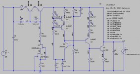
Sorry, I let spice re-number the components by default, as they got added. I will change that to be in sync with your schematic; will also change the component values.
The simulation statement is the same as yours .ac ...
You probably know this, but I will say it anyway, as it may help somebody else who does not.
There is an alternate way to calculate the output impedance, using this spice statement:
.tf v(out) v1
In ltspice choose from the menu Simulate->Edit Simulation CMD->DC Transfer, and fill in the two values, for the output use the output voltage (e.g. v(out) if you labeled "out" the output node), and for the input the voltage source you're using.
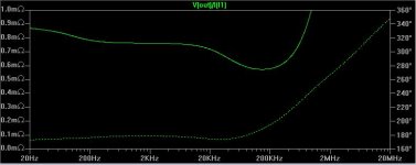
To get the output impedance bode plot against frequency, set the AC small signal value of the load to 1 (I noticed that you set it to 5m, or 1m, but it should not change the result), and run the .ac simulation. Then plot V(out)/I(I1), i.e. output voltage divided by the current of the load. To get this, plot V(out) first. Then in the bode plot window, click the right mouse button on the label V(out), and type in the dialogue window /I(I1) to the right of V(out). This will still show the plot in dB. Now click the left mouse button to the left of the X axis on the bode plot. A dialogue should open; choose "linear". The plot should now show Ohms on the left axis. In this same dialogue you can change the range of the X axis plot.
Hope this helps. Thanks for the led model; I did use that too (chased it last night in your earlier posts), but it did not bias the bjts correctly, perhaps because I have slightly different parts values here and there. I will sync my circuit to yours and try again.
The simulation statement is the same as yours .ac ...
You probably know this, but I will say it anyway, as it may help somebody else who does not.
There is an alternate way to calculate the output impedance, using this spice statement:
.tf v(out) v1
In ltspice choose from the menu Simulate->Edit Simulation CMD->DC Transfer, and fill in the two values, for the output use the output voltage (e.g. v(out) if you labeled "out" the output node), and for the input the voltage source you're using.
To get the output impedance bode plot against frequency, set the AC small signal value of the load to 1 (I noticed that you set it to 5m, or 1m, but it should not change the result), and run the .ac simulation. Then plot V(out)/I(I1), i.e. output voltage divided by the current of the load. To get this, plot V(out) first. Then in the bode plot window, click the right mouse button on the label V(out), and type in the dialogue window /I(I1) to the right of V(out). This will still show the plot in dB. Now click the left mouse button to the left of the X axis on the bode plot. A dialogue should open; choose "linear". The plot should now show Ohms on the left axis. In this same dialogue you can change the range of the X axis plot.
Hope this helps. Thanks for the led model; I did use that too (chased it last night in your earlier posts), but it did not bias the bjts correctly, perhaps because I have slightly different parts values here and there. I will sync my circuit to yours and try again.
C4 is interesting, 100uF across say 10 ohms dynamic impedance has a corner freq of about 1.5Hz. So, something in the order of a few 10's of uF might help.
Yabut ... C4 (or actually C3) and the reference are in parallel, so how do you calculate the corner frequency here? I was assuming the the impedance of the bypass cap should be as low or lower as the dynamic impedance of the voltage ref (some 6 - 10 Ohms for some zeners and for LEDs, lower for active Vrefs)? Btw., I have some old issues of AA with a 3 tier article on a superreg by the gentlemen Jung and Didden. They use 560µF in parallel to the voltage reference for to have a low enough impedance

MRupp said:
Yabut ... C4 (or actually C3) and the reference are in parallel, so how do you calculate the corner frequency here? I was assuming the the impedance of the bypass cap should be as low or lower as the dynamic impedance of the voltage ref (some 6 - 10 Ohms for some zeners and for LEDs, lower for active Vrefs)? Btw., I have some old issues of AA with a 3 tier article on a superreg by the gentlemen Jung and Didden. They use 560µF in parallel to the voltage reference for to have a low enough impedance
Yes, you calculate the frequency where f = 1/(2*pi*R*C) . That's your corner freq. I assumed 10 ohms for the dynamic zener Z, probably close enough to get an idea of how critical that cap is.
Was it 560uF? My, that's a lot. Don't remember the reasoning behind it, but I would user a lower value today. Or maybe it had something to do with the startup.
Jan Didden
r12 allows for 60V or 70V outputs and keep the voltage across the 245 CCS below max Vds. It may also damp any tendency to oscillate with spikes at the input.janneman said:
I don't think C5 is that critical, .........................
C4 is interesting, 100uF across say 10 ohms dynamic impedance has a corner freq of about 1.5Hz.....................wondering about R12, hadn't noticed it before. I guess *someone* had a good reason to put it in?
Iko's latest sim run seems to be showing that the shelf is not caused by C4 nor C5.
Which other C is causing this step? Surely not the output cap, that will be the dip at 100s kHz. Is it a C inside a semi?
what currents does the sim assume through all the components?
That might explain why variation in LED models is giving weird results.
The big problem I see is the low gain of the BD devices. When one takes these base currents into account then indeed weird voltages and currents start to pop up.
Do it manually to understand the DC operation.
That might explain why variation in LED models is giving weird results.
The big problem I see is the low gain of the BD devices. When one takes these base currents into account then indeed weird voltages and currents start to pop up.
Do it manually to understand the DC operation.
what currents does the sim assume through all the components? That might explain why variation in LED models is giving weird results.
Trust me, at least once, the standard LED model in spice does not give any meaningful results, its voltage drop is close to a standard diode, hence these variations. Read the article and try the adopted model for yourself. I found out when I tried to get another circuit working and the current did not match at all so that the circuit was basically not working. As for the bias current of the LEDs, I took care to have them at several mA in every sim that I did which was good enough for the 100 nA running thru the BDs.
I was just wondering about R12, hadn't noticed it before. I guess *someone* had a good reason to put it in?
That was me, I may need a higher voltage regulator (60V) and the idea is not to exceed the voltage rating and dissipation of the upper JFet (30V) - I presume there might be others who need higher voltages too. Can off course be shunted with a piece of wire.
MRupp said:
That was me, I may need a higher voltage regulator (60V) and the idea is not to exceed the voltage rating and dissipation of the upper JFet (30V) - I presume there might be others who need higher voltages too. Can off course be shunted with a piece of wire.
OK, in that case I would use a zener. If you have a transient input voltage before the CCS current gets up to speed you still will overload the Vds.
Jan Didden
AndrewT said:
r12 allows for 60V or 70V outputs and keep the voltage across the 245 CCS below max Vds. It may also damp any tendency to oscillate with spikes at the input.
Iko's latest sim run seems to be showing that the shelf is not caused by C4 nor C5.
Which other C is causing this step? Surely not the output cap, that will be the dip at 100s kHz. Is it a C inside a semi?
Andrew,
I think I see that with the higher C5 the increase at LF is not as large, 5m Ohms instead of going up to 12m Ohms. So I think there is definitely the C5 effect. Maybe others too.
Jan Didden
If you guys want to exclude the LED models in comparing your sims, just replace them temporarily with a 2.2V battery...
Jan Didden
Jan Didden
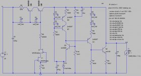
My apologies for the confusion in having posted the schematic with different part numbering. For the reference, this is the circuit (hopefully in sync with Martin's) that generated the plot in my previous post.
Edit: also, I should add. The value of C3 does not affect Zout in my simulation. A higher value of C1 lower the impedance in the range <= 200Hz.
Edit: also, I should add. The value of C3 does not affect Zout in my simulation. A higher value of C1 lower the impedance in the range <= 200Hz.
Attachments
I don't doubt your thoroughness.MRupp said:Trust me, at least once,
I can't remember what you found wrong with the LED models.
What are the (sim) predicted currents through all the components?
Using Martin's values, this is what I get:
--- Operating Point ---
V(in): 25 voltage
V(n3): 24.1317 voltage
V(out): 21.457 voltage
V(n1): 2.85952 voltage
V(n7): 0.0535013 voltage
V(n4): 22.5111 voltage
V(n2): 23.411 voltage
V(n5): 21.7905 voltage
V(n6): 14.9356 voltage
V(n18): 18.0052 voltage
V(n9): 9.06877 voltage
V(n10): 20.4393 voltage
V(n11): 17.3867 voltage
V(n12): 9.78402 voltage
V(n15): 0.686278 voltage
V(n16): 0.0285461 voltage
V(n17): 18.1156 voltage
V(n14): 18.0864 voltage
V(n19): 18.7134 voltage
V(n8): 19.7312 voltage
V(n13): 19.7863 voltage
Ic(Q1): -0.00501594 device_current
Ib(Q1): -1.47671e-005 device_current
Ie(Q1): 0.00503071 device_current
Ic(Q7): -0.00515128 device_current
Ib(Q7): -2.05693e-005 device_current
Ie(Q7): 0.00517185 device_current
Ic(Q4): -0.00517185 device_current
Ib(Q4): -2.04727e-005 device_current
Ie(Q4): 0.00519232 device_current
Ic(Q2): 0.0265646 device_current
Ib(Q2): 0.000113958 device_current
Ie(Q2): -0.0266786 device_current
Ic(Q3): 0.00516604 device_current
Ib(Q3): 7.80379e-006 device_current
Ie(Q3): -0.00517385 device_current
Ic(Q6): -0.147844 device_current
Ib(Q6): -0.000928939 device_current
Ie(Q6): 0.148773 device_current
Ic(Q5): -0.148773 device_current
Ib(Q5): -0.000930797 device_current
Ie(Q5): 0.149704 device_current
I(C1): 1.1673e-017 device_current
I(C3): 9.06876e-018 device_current
I(C2): 2.1457e-015 device_current
I(C4): 5.49999e-015 device_current
I(D5): 0.00503071 device_current
I(D6): 0.00503071 device_current
I(D4): 0.0102986 device_current
I(D2): 0.0102781 device_current
I(D3): 0.00241489 device_current
I(D1): 0.00148409 device_current
I(I1): 0.1 device_current
I(R9): 0.0266786 device_current
I(R7): 0.00490199 device_current
I(R8): 0.00503071 device_current
I(R10): 0.000770396 device_current
I(R4): 0.000778199 device_current
I(R1): 0.00519232 device_current
I(R2): 0.0103192 device_current
I(R5): 0.00334383 device_current
I(R3): 0.00334383 device_current
I(R6): 0.149704 device_current
I(V1): -0.151188 device_current
Ix(j1:10): 0.00334383 subckt_current
Ix(j1:20): -2.91359e-012 subckt_current
Ix(j1:30): -0.00334383 subckt_current
Ix(j3:10): 0.00334383 subckt_current
Ix(j3:20): -1.76889e-011 subckt_current
Ix(j3:30): -0.00334383 subckt_current
Ix(d14:1): -0.015493 subckt_current
Ix(d14:2): 0.015493 subckt_current
Edit: included node labes and voltage values.
Attachments
Hi,
the first problem that must be solved is the input CCS.
The hFE of the BD is modeled @ ~161 giving base currents of >0.9mA
Yes, more than half of the current through the J1 CCS comes from the bases of the transistors and only 44% of J1's CCS current flows through D1 LED.
But, it gets worse.
The BD's can have an hFE between 40 and 250. At the low hFE end this is a disaster. D1 could actually switch off, if a low hFE BD were selected for one or both BD140s
BD140 Q5 must be replaced with a high hFE device that can carry at least double your intended pass current. A suitable spec would be hFE>300 and Icmax>300mA.
BD140 Q6 must be selected for hFE >150 over the whole current range you intend to pass. A more suitable device should be found.
J1 needs to be >8mA Idss and R3 set to achieve at least 6mA through the FET CCS. A low pinch off voltage, high gm device is more suitable here (maybe k170bl).
If these changes are made the LED D1 current >=75% of the FET CCS current. The closer to 90% the better. I will certainly choose high hFE devices for Q5 & Q6 and use k170 for J1, but my max current is likely to be <=70mA and max load 20 to 40mA
2n6036 perhaps? I too would have preferred the 2sk170bl in that position.
Edit: never mind the 2n6036. The performance goes down the drain.
Edit: never mind the 2n6036. The performance goes down the drain.
AndrewT said:Hi,
the first problem that must be solved is the input CCS.
The hFE of the BD is modeled @ ~161 giving base currents of >0.9mA
Yes, more than half of the current through the J1 CCS comes from the bases of the transistors and only 44% of J1's CCS current flows through D1 LED.
But, it gets worse.
The BD's can have an hFE between 40 and 250. At the low hFE end this is a disaster. D1 could actually switch off, if a low hFE BD were selected for one or both BD140s
BD140 Q5 must be replaced with a high hFE device that can carry at least double your intended pass current. A suitable spec would be hFE>300 and Icmax>300mA.
BD140 Q6 must be selected for hFE >150 over the whole current range you intend to pass. A more suitable device should be found.
J1 needs to be >8mA Idss and R3 set to achieve at least 6mA through the FET CCS. A low pinch off voltage, high gm device is more suitable here (maybe k170bl).
If these changes are made the LED D1 current >=75% of the FET CCS current. The closer to 90% the better. I will certainly choose high hFE devices for Q5 & Q6 and use k170 for J1, but my max current is likely to be <=70mA and max load 20 to 40mA
Good points Andrew. I'm not sure that the BD Hfe has such a large spread though; normally one can order them in Hfe groups and I always order the highest group, which puts the Hfe min at 120 IIRC.
But it certainly is something to watch out for and as a minimum it's a good idea to increase the J1/J3 current as you proposed.
Jan Didden
Andrew,
Would you suggest a BD684 Darlington instead of the BD140, or perhaps a jfet (k170) driving a D45H11 (as per teddy-reg) or even perhaps a common fet (irfp610s)?
Would you suggest a BD684 Darlington instead of the BD140, or perhaps a jfet (k170) driving a D45H11 (as per teddy-reg) or even perhaps a common fet (irfp610s)?
another thread has used BIG mosfets for the pass in the CCS and the pass in the shunt.
There are some who say that the sound is better if the pass fets are replaced with BJTs.
If we only change the CCS bjt to fet, does the sound quality deteriorate?
If we use a small/medium power mosfet, does that help reduce or eliminate the degradation?
We are about to order thousands of boards, can we take the risk of too many unmeasurable alterations?
If it were not for that other thread I would change to bc550c + irf9610 in the ccs, but it is no longer a Cetoole. What attracted me initially were the small size and the superb posted sims of the Cetoole.
In general darlingtons are too slow, they are designed to save money on the production line, not for us.
- Status
- Not open for further replies.
- Home
- Amplifiers
- Solid State
- Bipolar discrete shunt regulators