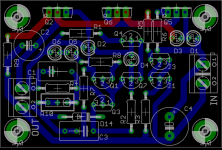
Email sent Jan
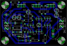
With the track sneaking under D2, it passed DRC with min clearance set at 12mils, but that's about it. The trace is 24mils currently, so I have changed it to 20mils (the one you have is 24mils with 12mil clearance).
At 20mils trace width, it now has 14mils clearance.
Resistors are type 207 - bend them close to the body and you should have no problems fitting the typical Vishay/Dale RN55 or some other 1/4-1/2 watt resistor
For the poly caps, they were 5mm grid 5x7.5mm. I have been able to move things slightly to get 7.5mm grid (5.2x10.6mm) and added an extra pad for the 5mm grid caps
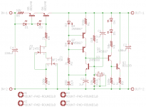
All numbering is consistent with Martin's schematic on post 280.
With the track sneaking under D2, it passed DRC with min clearance set at 12mils, but that's about it. The trace is 24mils currently, so I have changed it to 20mils (the one you have is 24mils with 12mil clearance).
At 20mils trace width, it now has 14mils clearance.
Resistors are type 207 - bend them close to the body and you should have no problems fitting the typical Vishay/Dale RN55 or some other 1/4-1/2 watt resistor
For the poly caps, they were 5mm grid 5x7.5mm. I have been able to move things slightly to get 7.5mm grid (5.2x10.6mm) and added an extra pad for the 5mm grid caps
All numbering is consistent with Martin's schematic on post 280.
Attachments
Looks impressive, Martin. How low can you go with R9 before you get oscillations
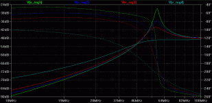
Jan, for the following diagram I set R8 (emitter resistor of Q1) to 50 and to 2 Ohms and R9 (emitter resistor of Q2) to 1 Ohms and 0.01 Ohms (basically no R9). I assume the peaks at high frequency are ctually showing potential resonances (?).
Vout1 (green): R8=50, R9=1
Vout2 (blue): R8=2, R9=1
Vout3 (red): R8=50, R9=0.01
Vout2 (light blue): R8=2, R9=0.01
Attachments
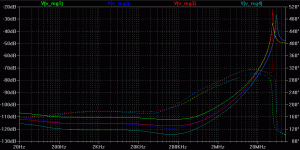
Here is a higher resolution of the peak area. I believe R8 can be low (a few Ohms) or even be omitted as the two LEDs would still have a combined dynamic impedance of ca. 12 Ohms (and LED bias is used in tube circuits). R9 may need more careful selection:
Attachments
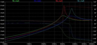
Now I have R8 fixed at 1 Ohm and R9 set to 0.01, 1, 2, 10 Ohms (green, blue, red, light blue). I presume this needs to be tested in the real circuit, maybe starting at 1 Ohm. Please note that the cap models were LTSpice models (Nichicon elco) without series inductance, adding a series inductance of say 20nH does not create new resonances but apparrently the caps are no longer effective at high frequencies:
Attachments
J1 must be low pinch of voltage. 245c is not suitable.
Hi Andrew,
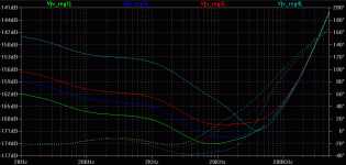
you are right, 245C is not very well suited in the lower position. Below diagram shows PSRR for different JFETs in the lower position, from top to bottom curve (Idss of the spice model): 245C (15.4 mA), 245A (3.95 mA), 245B (6.74 mA), and K170 (8 mA).
K170 is best but has a different footprint, and for the extra 3dB might not be worth it (noise I have not tested). Omitting the source resistor did not bring much improvement, I personally prefer to leave it in. Also, note that these are just the model values, in real life you get a spread of Idss values. Idss range from the BF245 datasheet: 245A: 2-6.5mA, 245B: 6-15mA, 245C: 12-25mA. A good compromise would be to choose BF245B, select for Idss, use the lower values at the bottom and the higher at the top.
Attachments
I have to actually correct myself. For the low pinchoff jfets K170 (8mA) and 245A (3.95mA) a source resistor did not change performance much. For the higher pinchoff models I do get a noticeable improvement with a source resistor. For 245B (6.74mA) 10-40 Ohms was about optimal, for the 245C (15.4mA) it was 600 Ohms. Obviously the value changes substantially, in simulation.
MRupp said:Now I have R8 fixed at 1 Ohm and R9 set to 0.01, 1, 2, 10 Ohms (green, blue, red, light blue). I presume this needs to be tested in the real circuit, maybe starting at 1 Ohm. Please note that the cap models were LTSpice models (Nichicon elco) without series inductance, adding a series inductance of say 20nH does not create new resonances but apparrently the caps are no longer effective at high frequencies:
Welcome to the real world!
The peaks in the earlier pics show indeed resonances, the giveaway is if you look at the phase curve where you see a jump of about 180 degrees at that point. That is a change of capacitive to inductive behaviour of the network. But it is at a fairly high freq, and since we expect this supply to handle only audio signals, we can live with it, unless it would lead to actual oscillations.
And as you say, these last few items need to be tested in practise since they depend very much on the part models.
Jan Didden
jameshillj said:Hang on yet, Twitchie.From post 282 (Cct and size of 21.6" (=60mm x 40mm) and scaling the components - some are quite small...Resistors = 7.4mm long X 2.5 ( -> 12mm?)Box Caps = 5.7 x 5mm @ 5mm pins ( -> 12 x 10mm?)I/P Cap = 8mm @3.5 mm pins (-> 10mm dia @ 3.75, 5mm)O/P Cap = 10mm @ 5mm pins (-> 15 dia @ 5,7.5mm)Power tracks of 60mils [1.5mm?] (-> 2.0mm)Not everyone will be using miniature components and increased size for the box caps allows for some different options.The bigger power tracks are for those boards that aren't 2 oz.I gather from your last post Jan, that you'll check tolerances and re-number the components?
Apparently the Design Rules have already been checked and found OK. I don't want to get involved with parts dimensions, but the early board I got some time ago had resistors standing up because they didn't fit, so this is definitely something to look into. I use 0.4inch (10mm) for my resistors and that handles pretty much all brands. LEDs have 0.1inch/5mm generally. Someone should check the cap dimensions and adjust the board if required.
And I NEVER chance part references on the board. If you want to do that (and I wouldn't know why you would), do it on the schematic and carry it forward to the board; the process should be automatic. It is absolutely vital to keep the board at 1:1 relationship to the schematic, or you end up with wrong boards, confusion, non-working boards and smoke escaping...
Jan Didden
twitchie said:Email sent Jan
With the track sneaking under D2, it passed DRC with min clearance set at 12mils, but that's about it. The trace is 24mils currently, so I have changed it to 20mils (the one you have is 24mils with 12mil clearance).
At 20mils trace width, it now has 14mils clearance.
Resistors are type 207 - bend them close to the body and you should have no problems fitting the typical Vishay/Dale RN55 or some other 1/4-1/2 watt resistor
For the poly caps, they were 5mm grid 5x7.5mm. I have been able to move things slightly to get 7.5mm grid (5.2x10.6mm) and added an extra pad for the 5mm grid caps
All numbering is consistent with Martin's schematic on post 280.
Looking good, but you may want to check R9/Q2 interference. if you want to bend Q2 backwards flat onto a heatsink or bracket, R9 is in the way. It's a bitch that R9, ain't it 😉 ?
One possibility: Move Q1 and Q3 a bit down, move R1 and R8 slightly up, move D2 between R8 and Q1, move R9 above R1....
Jan Didden
resistor pin pitch
0.3inch to 0.4inch is a big jump in pin pitch.
Use 0.35inch (8.9mm) for most metal films upto 600mW.
Can R9 be moved down, rotated maybe, beside C2?
Q5 does not need a heatsink, if that helps.
0.3inch to 0.4inch is a big jump in pin pitch.
Use 0.35inch (8.9mm) for most metal films upto 600mW.
Can R9 be moved down, rotated maybe, beside C2?
Q5 does not need a heatsink, if that helps.
Sorry to harp on this resistor and capacitor size thing but this pcb design is supposed to be a "Universal" to suit a number of different requirements.
So, restricting the size of the first input resistor (R6?) to 7.5mm (and close proximity to the transistor) for example, limits the power thru the device, and so on.
And it's never good practice to "bend sharp" the component leads.
Sorry to be such a negative and critical person after all your good work Twitchie, but there are about 1300 of these pcbs on the Wiki list intended for a wide variety of uses and components so as many options as can be included would be a priority
The peaks in the earlier pics show indeed resonances
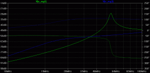
I think R8 is not necessarily needed now to drop more voltage. However, one way to tame possible resonances is to replace R8 with a small (0207 resistor size) inductance of ca. 1 - 5 µH and high enough self resonance of say 100 MHz or above (cost 25 Euro-cent at a local supplier). Attached chart is with R9 =0.01 Ohms, green curve with R8 = 2 Ohms, blue curve with R8 replaced by 3.3 µH (btw., performance up to 100KHz seems identical):
Attachments
AndrewT said:is Twitchie's PCB for his own use or is this the proposal for the Group Buy?
I don't know if it changes the cost of producing boards or not, but the reason why I've been struggling with placements and trace routing is because this board is single layer still. I wanted to be able to etch this and a dual layer board would need to go to a fab (or require a dedicated individual to home-etch it) before it could be tested.
My hope was that at least we could test the circuit and if nothing else came up, it could be used for the GB, but I'm doing this for fun and as a good learning exercise. I would have no objections and would not be offended if someone else offered up their own layout.
If nobody has any concerns, I'll start moving traces to the top layer, switch resistor package to 207-10 (10mm) and if board dimensions aren't affect too much, I'll see if 15mm lead caps will fit C1/C3
Example: DS board at this size, with top silk screen and through-metallised holes will be less than 3 euro's each at 100 pieces at my board maker, including shipping (single shipment) to an address in Europe. Not sure this includes Scotland 😉 .
Jan Didden
Jan Didden
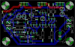
- moved a few traces to top layer
- 207-10 (10mm) resistor package used now
- current board size is 2500milsx1550mils (2.5x1.55 inch)
- not going to attempt 15mm lead space poly caps
- not thrilled with the 1 pad of R8 at the corner of C1 (going to play with it a bit)
- had to merge the output of D2 and R1 a bit sooner than previous
Attachments
If you're not yet sick of this:
Move the following to the left:
Q2 Q6 Q5
D3 D1
R3 C4
Then the input connector into the hole toward the left, then the two right mounting holes to the left, and your board becomes even smaller = cheaper...
Jan Didden
Move the following to the left:
Q2 Q6 Q5
D3 D1
R3 C4
Then the input connector into the hole toward the left, then the two right mounting holes to the left, and your board becomes even smaller = cheaper...
Jan Didden
The input connector is just pushed to the edge arbitrarily. It's the mounting holes that constrains the board at this size - the mounting holes can only go as far as Q5, D3 and C4 - Q5 is constrained to the left by R5/R6 and those are constrained by J3, which is constrained by ... and so on
I could probably squeeze out another 50 mils or so, but that's about it ... I'll keep thrashing this one around and see if there's a solution
Definitely keep the suggestions coming though. More eyes are always welcome
P.S. Yes, I did consider pushing the CCS down, to move R5 and R6 out of the way, but then you lose the ability to push C4, so no net gain to be had on the bottom
- Status
- Not open for further replies.
- Home
- Amplifiers
- Solid State
- Bipolar discrete shunt regulators