jameshillj said:...And it's never good practice to "bend sharp" the component leads.
I entirely agree. I use a pair of needle pliers (with the sharp edge ground to create a bend radius) to grip the lead near the body, then make the bend = no stress. It's so ugly bending from the body. Thus 0.4" on a 1/4W is about minimum.
Brian.
I need to apologize to all the people who contributed to this effort who may have been missed in the 'Thank You' line I put in the last image. I'm going to take the line out just to be fair to everyone, but I think we all need to recognize the efforts by Apassgear, Steenoe and Manu all especially to get us to where we are today.
Thanks guys and sorry for missing your names. I'm sure everyone appreciates all your efforts and I think it deserves to be mentioned again.
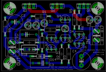
Latest changes:
- moved D1 and D3 to the left to shorten those traces
- made a single layer version for etching/testing but requires 1 jumper at R5 and not shown on the layout but the holes are there
I'm attaching the pdfs for etching if someone wants to build/test this in single layer form - copper is not mirrored, silk layer is mirrored
Thanks guys and sorry for missing your names. I'm sure everyone appreciates all your efforts and I think it deserves to be mentioned again.
Latest changes:
- moved D1 and D3 to the left to shorten those traces
- made a single layer version for etching/testing but requires 1 jumper at R5 and not shown on the layout but the holes are there
I'm attaching the pdfs for etching if someone wants to build/test this in single layer form - copper is not mirrored, silk layer is mirrored
Attachments
twitchie said:[snip]I'm going to take the line out just to be fair to everyone[snip]
Good move. This was truly a group effort, and the board isn't large enough to list all contributors 😉
Jan Didden
BF244A is almost the same as BF245A.
The pin out is different and different between manufacturers.
The pin out is different and different between manufacturers.
The board looks real good.  I like that R5 and R6 were moved away from the power transistors. Thanks for all the effort that you have put into this layout.
BDP
I like that R5 and R6 were moved away from the power transistors. Thanks for all the effort that you have put into this layout.BDP
janneman said:It's almost looking like a board I would have designed 😀
Jan Didden
BDP said:The board looks real good.
BDP
😀 thanks for the kind words and thanks for your helpful emails BDP.
moving the resistors was Jan's idea

@ikoflexer - sorry I didn't get to reply to your earlier post - today was freezing ... this weather is driving me crazy


Q2 and Q6 need at least 20C/W heatsinks.
If you go for more current and/or more input voltage then big sinks may be needed.
If you go for more current and/or more input voltage then big sinks may be needed.
Layout - R1
Hello Twitchie,
I was playing with the layout and am confused by your schematic in post 302 versus the layout in post 322. Is there not a connection missing from the current source (collector of Q6) to the rest of the circuit, like R1, D2, etc.. Something looks not quite right? Or is this the wrong layout ? 😕
Q6 connects to Q2 then to out terminal.
The measuring side taps into the out terminal and not off the current delivery route/trace.
The measuring side taps into the out terminal and not off the current delivery route/trace.
My bad, I can see it now - hmmm, I swear when I looked at the board before it was not there ....
These are the things that happen if you break the link between schematic diagram and layout... (Yes sometimes I'm a PITA 😉 ).
Jan Didden
Jan Didden
- Status
- Not open for further replies.
- Home
- Amplifiers
- Solid State
- Bipolar discrete shunt regulators