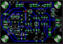
Are we there yet? I redid a few of the tracks. Couldn't figure out how to space out the cramped components R3/R4/C4 etc - the extra LED and the pot on R3 together gave me alot of trouble.
Current board size is 2.375x1.6. I never liked R10 up there either, but I was thinking it could be mounted underneath to avoid any heatsink issues on Q1
Ignore the missing tracks on the pot/R3 - they're in there now
Current board size is 2.375x1.6. I never liked R10 up there either, but I was thinking it could be mounted underneath to avoid any heatsink issues on Q1
Ignore the missing tracks on the pot/R3 - they're in there now
An externally hosted image should be here but it was not working when we last tested it.
An externally hosted image should be here but it was not working when we last tested it.
I'm trying to catch up with the thread... but I'm curious if the capacitor trick was tried, connecting the negative pin of C1 to in between LED2 and R8?
ikoflexer said:I'm trying to catch up with the thread... but I'm curious if the capacitor trick was tried, connecting the negative pin of C1 to in between LED2 and R8?
Well, you need C1 where it is. You could put an additional C where you mention it, but it's effect will be very marginal. It would need to be large to have any effect in parallel of the diodes which already have a very small dynamic impedance anyway.
On the board layout: I think you guys are now going around in circles. Fix the circuit as it is, and clean up the board if necessary, but basically it is OK. What I would do is to make the tracks that carry no current like those to/from the reference and feedback components much thinner, 15 mills is a good width. Eagle should have a simple way to click on a track and set the width. This will give you lots of room for the other ones that do need to be thicker, and will let you clean up the board.
Another point that needs to be done is to move the component labels so that they can be read when the board is populated. Some are now hidden (D3, R3, R4 etc) or even outside the layout area (R10, IN). Again, Eagle should allow you to (right) click either the component or the label and move it. Also, put a project name and board revision number on the silkscreen.
Jan Didden
Hi Mrupp,
post 280 shows J1=bf245c.
post 282 shows J1=bf245a.
J1 must be low pinch of voltage. 245c is not suitable.
a low pinch off voltage FET here will pass ~ 60 to 70% of it's Idss.
The LED current does not need to be precisely set, I guess anywhere between 2 and 4mA would do.
Choose a 3mA to 6mA Idss device for J1. Then the 100r (R3) can be deleted.
What happens if R2 is connected to ground as originally?
AndrewT said:[snip]What happens if R2 is connected to ground as originally?
Andrew, you mean R5?
Jan Didden
post 280 R2.
post 282 is bastardised due to changing most of the component numbers and changing many of the components.
post 282 is bastardised due to changing most of the component numbers and changing many of the components.
AndrewT said:post 280 R2.
post 282 is bastardised due to changing most of the component numbers and changing many of the components.
OK, I see. The idea of returning the resistor to the top of the ref is to have a more constant bias current through the ref. The transistor current will vary, and with that the ref current and thus the ref voltage. With the additonal (constant) current from R2, Iref and thus Vref varies less.
Small thing, admitted, but it will help and is free.
Jan Didden
janneman said:
OK, I see. The idea of returning the resistor to the top of the ref is to have a more constant bias current through the ref. The transistor current will vary, and with that the ref current and thus the ref voltage. With the additonal (constant) current from R2, Iref and thus Vref varies less.
Small thing, admitted, but it will help and is free.
Jan Didden
So please correct me if I misunderstand, but we WANT R2 connecting into the top of RF1/D3 to provide additional (constant) current to average out current variation, resulting in less voltage variation?
I'll revert that minor change back out once I get confirmation.
With respect to shrinking traces, I haven't a clue as to how much each trace carries, so if someone wants to point out which ones could be modified, I'll apply the updates, but if it's not going to provide much improvement, then I'm just as happy to leave them as they are.
Awaiting orders Captain ...

Good morning twitchie 🙂 nice day in TO
I have a bit of a puzzle on my hands because of an experiment I have done last night and perhaps some of the more experienced users can opinionate. Maybe this is old news, but to me the results were surprising. I setup a circuit like this:
batt -12V --- LED --- output --- variable resistor --- batt +12V
Connected a noise amp to the output point via a 1M resistor (to -12V) and a 0.1uF series cap, and then the output of the amp to the oscilloscope. Set the variable resistor so that 10mA passes through all parts tested (the LED was replaced with other parts for testing).
Most LEDs measured at about 100mV/div, red, green, yellow. All zeners (tried 5.1 and 6.2 V) measured around 500mV/div. A transistor B-E connected, about 200mV/div. Regular diodes (e.g. 1n4006) also about 200mV/div. Now, if this does not surprise you, perhaps the next bit will. We have seen circuits around here which use a capacitor in parallel with the LED. The larger the capacitor value, the larger the noise; for example, a 220uF cap would raise the noise of the LED from 100mV/div to about 700mV/div.
How about connecting the capacitor to the output point via a 500R resistor, i.e. output --- 500R --- output1 --- 220uF --- batt -12V thus setting up a filter; the noise was measured at point output1. Various values of capacitor and resistor did not help in reducing the LED noise.
In summary, the lowest measured noise was of single red/yellow/green LEDs.
For current carrying traces just follow both legs of the raw supply input through the power tranies collector and emitters and end up on the output connector. You may consider all other traces as low current ones including the ones going to the bases of the power tranies.
Yes, according to Jan you should connect R5 as shown on schematic on post 282.
Cheers,
Yes, according to Jan you should connect R5 as shown on schematic on post 282.
Cheers,
A good rule of thumb: any trace that leads to a resistor of several 100 ohms or more CANNOT carry a lot of current, so a narrow trace is OK.
Jan Didden
Jan Didden
ikoflexer said:Good morning twitchie 🙂 nice day in TO
I have a bit of a puzzle on my hands because of an experiment I have done last night and perhaps some of the more experienced users can opinionate. Maybe this is old news, but to me the results were surprising. I setup a circuit like this:
batt -12V --- LED --- output --- variable resistor --- batt +12V
Connected a noise amp to the output point via a 1M resistor (to -12V) and a 0.1uF series cap, and then the output of the amp to the oscilloscope. Set the variable resistor so that 10mA passes through all parts tested (the LED was replaced with other parts for testing).
Most LEDs measured at about 100mV/div, red, green, yellow. All zeners (tried 5.1 and 6.2 V) measured around 500mV/div. A transistor B-E connected, about 200mV/div. Regular diodes (e.g. 1n4006) also about 200mV/div. Now, if this does not surprise you, perhaps the next bit will. We have seen circuits around here which use a capacitor in parallel with the LED. The larger the capacitor value, the larger the noise; for example, a 220uF cap would raise the noise of the LED from 100mV/div to about 700mV/div.
How about connecting the capacitor to the output point via a 500R resistor, i.e. output --- 500R --- output1 --- 220uF --- batt -12V thus setting up a filter; the noise was measured at point output1. Various values of capacitor and resistor did not help in reducing the LED noise.
In summary, the lowest measured noise was of single red/yellow/green LEDs.
If I read you correct you use the LED in series mode. In that case, you don't measure the LED noise but the current noise in the total circuit. If you parallel the LED with a cap you change the current noise but it doesn't say anything abut the LED voltage noise, which is important for reference purposes.
BTW Reporting in 'xxxmV/div' doesn't tell us anything, the actual value is the number of divisions * mV/div. So if you have 100mV/div and see 8 divisions that's 800mV, with 500mV/div and 1 cm its only 500mV.
Jan Didden
janneman said:
If I read you correct you use the LED in series mode. In that case, you don't measure the LED noise but the current noise in the total circuit. If you parallel the LED with a cap you change the current noise but it doesn't say anything abut the LED voltage noise, which is important for reference purposes.
Yes, the LED is in series with a resistor, and the measuring point is in between them. Should the setup be different to measure voltage noise at that point? I agree that is is the circuit noise that is measured there, but it can it can still be used for comparison can it not? I did not want to touch absolute measurements because nothing I have is calibrated. However, it is consistent in its non-calibration, i.e. the measurements are reproducible.
Also, if we parallel the LED with a cap, which I have done because it is seen in several schematics, the noise of the circuit thus made is of interest. You are right, it says nothing about the noise of the LED, but it tells us about the noise of the two paralleled. The noise is larger. It was my understanding that some people used this to "filter" (reduce) the LED noise somewhat; I see evidence that the contrary is true.
I also described another setup, with a real filter similar to that employed by Walt Jung in his regulator, R-C (499R, 120u he uses, or similar values) to filter zener noise. This also did not change the peak-to-peak values that I have seen on the scope.
Granted, perhaps there is so much noise in the circuit that the LED noise is just buried in the rest of the noise. However, this is not the case, since the noise increases/decreases depending on the component tested; the other indication is that I have also used a resistor as the component tested (component value chosen for 10mA) instead of the LED, and the p-p values were much lower.
BTW Reporting in 'xxxmV/div' doesn't tell us anything, the actual value is the number of divisions * mV/div. So if you have 100mV/div and see 8 divisions that's 800mV, with 500mV/div and 1 cm its only 500mV.
Jan Didden
Oops, you're right, this is my mistake. Basically, to translate the values I reported, the oscilloscope was set to 100mV/div and the values I reported should not be read as /div. For instance, the noise peak-to-peak for a red LED in the circuit was 100mV, or 1 div.
As I said, this may be old news here, but it was unexpected for me. Please let me know, if there is anything you think I should change in the test setup, if it is of any interest to you.
I plan to test the regulator designed here with this setup and possibly compare with other regulators. Incidentally, the noise I could see on the utility line ground connector is p-p almost equal to one red LED noise in the circuit above. The oscilloscope pattern does differ, but the p-p values are very close (with the ground noise being a bit smaller value).
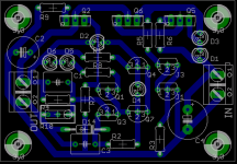
Well done. That underpass at D2 did it.
Now, do you know what the Design Rule setting for this board is? The DR specifies the allowed clearance between track-trac, track-pad and pad-pad. If you violate this, the program will give an error message.
You may want to check that to see that the celarance at D2 is at least 12 or 15 mills to avoid problems with the final board. Click the DRC-icon, then the cClearance tab.
Can you email me the board .brd file, I'll check it, jan123didden01@gmail123.com, delete all numbers except the 01.
Jan Didden
Hang on yet, Twitchie.From post 282 (Cct and size of 21.6" (=60mm x 40mm) and scaling the components - some are quite small...Resistors = 7.4mm long X 2.5 ( -> 12mm?)Box Caps = 5.7 x 5mm @ 5mm pins ( -> 12 x 10mm?)I/P Cap = 8mm @3.5 mm pins (-> 10mm dia @ 3.75, 5mm)O/P Cap = 10mm @ 5mm pins (-> 15 dia @ 5,7.5mm)Power tracks of 60mils [1.5mm?] (-> 2.0mm)Not everyone will be using miniature components and increased size for the box caps allows for some different options.The bigger power tracks are for those boards that aren't 2 oz.I gather from your last post Jan, that you'll check tolerances and re-number the components?
Hang on yet, Twitchie.From post 282 (Cct and size of 21.6" (=60mm x 40mm) and scaling the components - some are quite small...Resistors = 7.4mm long X 2.5 ( -> 12mm?)Box Caps = 5.7 x 5mm @ 5mm pins ( -> 12 x 10mm?)I/P Cap = 8mm @3.5 mm pins (-> 10mm dia @ 3.75, 5mm)O/P Cap = 10mm @ 5mm pins (-> 15 dia @ 5,7.5mm)Power tracks of 60mils [1.5mm?] (-> 2.0mm)Not everyone will be using miniature components and increased size for the box caps allows for some different options.The bigger power tracks are for those boards that aren't 2 oz.I gather from your last post Jan, that you'll check tolerances and re-number the components?
- Status
- Not open for further replies.
- Home
- Amplifiers
- Solid State
- Bipolar discrete shunt regulators