No, you would do better with a B1, or DCB1, or a Juma style style Buffer, or even a Juma style preamp with gain.
If you need a preamp go with the 3 BF862 preamp that I made following Juma's design on this thread. It's a very nice sounding preamp with gain.
See post #346Hi X,
Can I simply chop off the LU1014D and use the BF862 part as a gain stage for my DCB1?
Those who have already built B1 and just need some additional gain, can add just the gain stage (and the PSU) in the existing box. Coupling cap (C3) is not needed if your B1 already has one at the input.
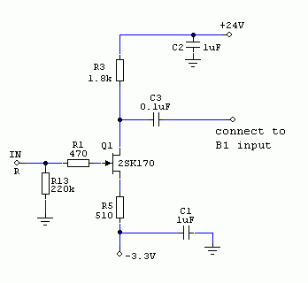
I want to add a gain stage to the existing DCB1 that I am using and I saw the above which looks possible, I want to try BF862 instead of K170 but using the single rail power supply instead.
Juma,
Thanks for your reply, so I can just use it as it is or strip the Q2 and Q3 section ?
Thanks
Will use it with DCB1 driving a M2 and also Vfet2.
The DCB1 PS rail is 10.6x, sources is from a R2R dac output about 1.4 RMS.
The DCB1 PS rail is 10.6x, sources is from a R2R dac output about 1.4 RMS.
Will use it with DCB1 driving a M2 and also Vfet2.
The DCB1 PS rail is 10.6x, sources is from a R2R dac output about 1.4 RMS.
To max out an M2 you need ca 4Vpk. Thats 8V swing on the output. 1.4 V RMS is 2Vpk, so you are looking for a gain of two, maybe a little more. Around the post cited by Juma above you find info on setting the gain.
I didn't get what your supply voltage at the top of R5 is going to be. If it is a lot lower than 24V you may want to adapt R5, R2, R3 to get a useful result.
Also knowing the Idss of your BF862 helps to choose said resistors.
My PS will be +24V going into Juma's Cap multipler ending up with roughly 22V, I am looking at somewhere of 9db gain or 2.X should be more than sufficient. I didn't measure the Idss on the BF862 yet, will try to by end of the month.
Thanks
Thanks
22Vdc supply allows a no load maximum output of roughly 7Vac
If you attach a high impedance load that maximum output drops a little bit, maybe 6Vac to 6.5Vac.
Attaching a low impedance load that is still within the drive specification could drop the maximum output down to around 6Vac
A single ended no global feedback amplifier begins to increase distortion as it approaches 50% of maximum output. And the distortion increases massively as the output approaches 100% of maximum.
On this basis I have recommened that our normal maximum signal through the amplifier should be limited to <50% of the actual amplifier max. i.e. for a 22Vdc supply to a single ended no global feedback amplifier driving a low impedance load aim to use no higher than 3Vac and maybe around 3.5Vac, when the loading is high impedance.
2.8Vac (= 4Vpk) is only 40% of the high impedance maximum signal. 22Vdc is plenty.
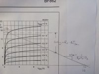
You can do your own loadline by looking at the data sheet.
In the given lineup the supply voltage Vs drops over the jfet (=Vds) and the resistors R5, R2, R3. So we have
Vs = Vds + Id * (R5+R2+R3),
with Id being the drain current.
This is the straight line in the Id(Vds) diagram.
It hits Id=0 at Vds=Vs and has a slope of 1/(R5+R2+R3).
All you need to do now is to choose your minimum Vds (common wisdom is to use 2*Vpinchoff=ca 1.3V for a BF862) and your maximum Vgs (people avoid positive values), this gives you your loadline and a value for (R5+R2+R3).
To find the Q-point you need to know your maximum output swing.
The output voltage swings because with changing Id also the voltage drop over R5 changes, the magnitude simply given by DeltaVout=R5 * DeltaId.
The Q-point is in the middle of that swing.
To get there you need to choose the quiescent Vgs for the JFET (read from diagram) and set it via Vgs = R2 * Id.
Lastly, the gain is approximately R5/(R2+R3+Rjfet), where Rjfet is 1/yfs as it is called in the datasheet. Datasheet says 40mS which would mean Rjfet=25Ohm, but this is meant for Vgs=0. Biasing the jfet down brings up Rjfet, probably to something like 35Ohm. No big factor in setting the gain, though.
The device shown in the datasheet has an Idss of over 17mA. If your Idss differs you need to adapt. Now you can go fiddle ...
Attachments
You can do your own loadline by looking at the data sheet.
In the given lineup the supply voltage Vs drops over the jfet (=Vds) and the resistors R5, R2, R3. So we have
Vs = Vds + Id * (R5+R2+R3),
with Id being the drain current.
This is the straight line in the Id(Vds) diagram.
It hits Id=0 at Vds=Vs and has a slope of 1/(R5+R2+R3).
All you need to do now is to choose your minimum Vds (common wisdom is to use 2*Vpinchoff=ca 1.3V for a BF862) and your maximum Vgs (people avoid positive values), this gives you your loadline and a value for (R5+R2+R3).
To find the Q-point you need to know your maximum output swing.
The output voltage swings because with changing Id also the voltage drop over R5 changes, the magnitude simply given by DeltaVout=R5 * DeltaId.
The Q-point is in the middle of that swing.
To get there you need to choose the quiescent Vgs for the JFET (read from diagram) and set it via Vgs = R2 * Id.
Lastly, the gain is approximately R5/(R2+R3+Rjfet), where Rjfet is 1/yfs as it is called in the datasheet. Datasheet says 40mS which would mean Rjfet=25Ohm, but this is meant for Vgs=0. Biasing the jfet down brings up Rjfet, probably to something like 35Ohm. No big factor in setting the gain, though.
The device shown in the datasheet has an Idss of over 17mA. If your Idss differs you need to adapt. Now you can go fiddle ...
Thanks for both ElFishi and AndrewT's clear explanation.
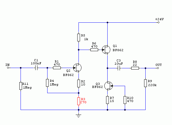
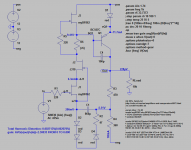
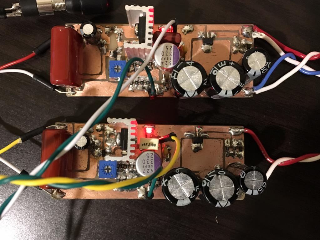
BF862 CFP preamp with servo
I have been playing around with the BF862 to find configurations with some gain and no coupling caps. Also I wanted to test the idea of a CFP for low Zout.
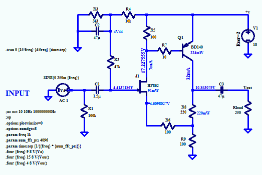
Here is a little circuit I put together and it works.
It uses a BF862 as input device, cascoded to keep Vds lowish and stable. CFP is done with a BC560 (Q1, in the sim I use BC557). Bias current is ca 12mA determined by the sum of R3 and R4. Gain comes from (R3+R4)/R4 and is 7.2dB. I guess you can turn this circuit into a head amp by using a bigger Q1 (like BD140) and going down in R3+R4, but I haven’t tried.
JFET bias is set by D2 – D4 plus R2. You can use a larger R2 instead of D2 – D4. The diodes, however, make C1 charge faster on startup. And they shine. (Btw, does anyone have experience with blue leds to drop voltages in audio circuits?). In the present gain setting R2 = 47 Ohms gives a Q-point of Vgs=-0.2V (Id=6.3mA with Idss=15mA), the THD sweet spot in simulation.
The CFP has an active load Q2 (BC560, too) biased by an OpAmp servo to regulate the output DC near zero. First low pass filter is R7/C2, second LPF is R6/C3 to keep all gunk away from the base of Q2.
D1 is there to increase Vce at Q2.
THD is 0.004% in simulation when delivering 4Vpk at 1kHz at the output. Simulated Zout is ca 3Ohm.
The OpAmp model for the TL071 I took from the ST website, I only had to change the pin assignments to
.SUBCKT TL07x 2 1 4 5 3
to match the OpAmp2 symbol of LTSPICE.
The model I found on the TI website gave me the problem that the sum of currents of all OpAmp terminals wasn’t zero.
For BF862 I use my own model parameters. Red led models come from Bob Cordell.
Comments solicited.
I have been playing around with the BF862 to find configurations with some gain and no coupling caps. Also I wanted to test the idea of a CFP for low Zout.
Here is a little circuit I put together and it works.
It uses a BF862 as input device, cascoded to keep Vds lowish and stable. CFP is done with a BC560 (Q1, in the sim I use BC557). Bias current is ca 12mA determined by the sum of R3 and R4. Gain comes from (R3+R4)/R4 and is 7.2dB. I guess you can turn this circuit into a head amp by using a bigger Q1 (like BD140) and going down in R3+R4, but I haven’t tried.
JFET bias is set by D2 – D4 plus R2. You can use a larger R2 instead of D2 – D4. The diodes, however, make C1 charge faster on startup. And they shine. (Btw, does anyone have experience with blue leds to drop voltages in audio circuits?). In the present gain setting R2 = 47 Ohms gives a Q-point of Vgs=-0.2V (Id=6.3mA with Idss=15mA), the THD sweet spot in simulation.
The CFP has an active load Q2 (BC560, too) biased by an OpAmp servo to regulate the output DC near zero. First low pass filter is R7/C2, second LPF is R6/C3 to keep all gunk away from the base of Q2.
D1 is there to increase Vce at Q2.
THD is 0.004% in simulation when delivering 4Vpk at 1kHz at the output. Simulated Zout is ca 3Ohm.
The OpAmp model for the TL071 I took from the ST website, I only had to change the pin assignments to
.SUBCKT TL07x 2 1 4 5 3
to match the OpAmp2 symbol of LTSPICE.
The model I found on the TI website gave me the problem that the sum of currents of all OpAmp terminals wasn’t zero.
For BF862 I use my own model parameters. Red led models come from Bob Cordell.
Comments solicited.
Attachments
I expect your cascode JFET is actually an MMBFJ310 in SMD packaging. The thru-hole J310 is only available from obsolete-part sellers like Rochester and Quest, at least according to to the search engine octopart.com: <<search results>>
I have been playing around with the BF862 to find configurations with some gain and no coupling caps. Also I wanted to test the idea of a CFP for low Zout....
guess you can turn this circuit into a head amp by using a bigger Q1 (like BD140) and going down in R3+R4, but I haven’t tried.
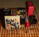
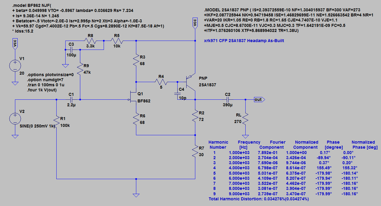
I have built Aksa's CFP headamp using BF862 on the front and 2SA1837 on the back. Sounds marvelous.
More info here:
http://www.diyaudio.com/forums/solid-state/301164-mosfet-source-follower-headamp-34.html
Looks like this:
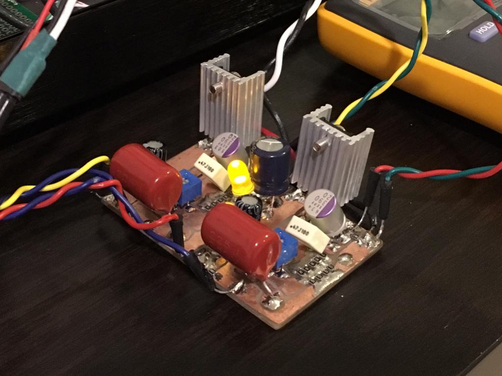
And here is one with BD140 (with on-board cap Mx using SMT MOSFET - which is nice as only 1.9v dropout):
- Home
- Amplifiers
- Pass Labs
- BF862 Preamp