AndrewT said:Idss ~10mA.
a little into the BC base.
Therefore ~10.02mA through the Zener.
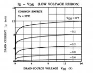
So there's about 0.5V across the FET. Does that work as a cs with such a low Vds? I'm not a FET man, but seems quite low.
Jan Didden
I have used this particular JFET taking advantage of 2 things. 1: It's one of the few that can can have lower pinch off voltage than a BJT's VBE. It actually fills the Jung's criteria for double pinch off there too. 2: Many left overs would be available after the matching process for those who made my NJFET open loop simplistic phono. And that simplistic shunt was developed for that phono. As a partner.
what's the pinch off voltage of a 10mAIdss k170?
what is double that voltage?
add on the 100mV across the 10r.
Does that really meet Walt's criteria?
what is double that voltage?
add on the 100mV across the 10r.
Does that really meet Walt's criteria?
Yes. That is why I use only 10R. 0.2V pinch off I have measured. Double that and add 0.1V. Also I measure 0.66V from Q3's base to GND. Walt said that is better to have double the pinch off headroom for best noise performance. It would work marginally even, but not best.
janneman said:
So there's about 0.5V across the FET. Does that work as a cs with such a low Vds? I'm not a FET man, but seems quite low.
Yes. For Vds=0.5V a 2SK170 is most likely in the saturation region (where it acts as a CCS). Incipient saturation is defined as the region where Vds>Vp 2SK170 has Vp=-0.2...-1.5V so Vds=0.5V will do.
It is unclear to me though what would be the advantage of this regulator. The loop gain looks pretty small (essentially gm(Q3)*R6~40dB, because the ratio between the dynamic impedances of the zener and the JFET CCS is almost 1) so the line regulation and output impedance are not very good.
Its not great. I am no engineer. I just test my DIY ideas. A shunt reg can be surely done technically better.
My criteria, was: Simple, no loop feedback, JFETS and Mosfets, much better sound than battery or LM317.
I did it and met my criteria. Then it has been implemented along my phono by so many people that report it dead silent and great sounding so its ok in my book.
My criteria, was: Simple, no loop feedback, JFETS and Mosfets, much better sound than battery or LM317.
I did it and met my criteria. Then it has been implemented along my phono by so many people that report it dead silent and great sounding so its ok in my book.
salas said:Its not great. I am no engineer. I just test my DIY ideas. A shunt reg can be surely done technically better.
My criteria, was: Simple, no loop feedback, JFETS and Mosfets, much better sound than battery or LM317.
I did it and met my criteria. Then it has been implemented along my phono by so many people that report it dead silent and great sounding so its ok in my book.
Well, I got some bad news for you 🙂 It has negative feedback, and about 40dB! The negative feedback loop is defined by the dynamic impedance of the zener and the impedance of the JFET CCS. The ratio is very small, so the loop gain is essentially the gain of the base amp (Q3) and the whole thing works as a unity gain amp, or Vo~Vz.
BTW, I am sure it sounds great 🙂
Damn I was expecting that there will be nesting somewhere!
I tried not to define some global feedback loop using op amps with gain etc.
I tried not to define some global feedback loop using op amps with gain etc.
I would think that using the current source in the place of R6 would immediately give a huge gain in loop gain and a huge gain in performance. The 10 ohms would then need to be like 60 ohms, of course.
Syn08, what do you think?
Jan Didden
Syn08, what do you think?
Jan Didden
Gimme your best upgrading ideas and I will surely try them. But I forewarn you...My top criteria is always that elusive anti engineering sanity, non cross checked thing, ''sounds better or not''.🙂
janneman said:I would think that using the current source in the place of R6 would immediately give a huge gain in loop gain and a huge gain in performance. The 10 ohms would then need to be like 60 ohms, of course.
Syn08, what do you think?
Jan Didden
Of course, another JFET instead of R6 will likely work much better. It will be at Vds = Vgs(on) Q4 which should be fine (it's a few volts). A nice simulation exercise, unfortunately I'm pretty tied right now... Loop stability should also be checked, unity CL gain with high OL gain things can get tricky...
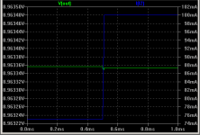
Bonsai said:Looking at your last post, if I'm reading it correcly I'd say you have problems. There should be no overshoot or ringing.
First, let me thank you for the stimulating conversation.
I think the entire power system needs to be addressed when looking at these regulators. For example, in the project I am working on today, there is a Jung-type regulator, but there is also an array of 8 39µF OS-CON caps, 8 1µF ceramic caps, and an 800pF capacitance due to the ground planes of the PCB. Output impedance of the whole system is < 100mΩ out to 80MHz and < 1Ω out to 400MHz, which I think is acceptable considering the passband only extends to 96kHz.
Regarding your comment, I agree the ringing was excessive in the plot I posted. It turns out that the AD825 has far better transient behavior than the AD820 (in simulation). I use the AD820 for low voltage outputs since it can swing rail-to-rail and run from a single 5V supply, and I use the AD825 for outputs ≥ 9V.
As you can see from this plot, the transient load response is rather good. For a (quite improbable) 25mA load step with a 10µs rise time, the output swings only about 10µV. That's -68dB @ 100kHz.
Attachments
jwb said:
Regarding your comment, I agree the ringing was excessive in the plot I posted. It turns out that the AD825 has far better transient behavior than the AD820 (in simulation). I use the AD820 for low voltage outputs since it can swing rail-to-rail and run from a single 5V supply, and I use the AD825 for outputs ≥ 9V.
I think that ADI posited 2 SPICE models for the AD825 depending upon the rail voltages.
True, but the models are for ±5 and ±15. Because of the 825's limited output swing, it's impractical to use it below 9V output. The 820, on the other hand, will swing down to the negative rail, so you can use it for a 5V regulator.
ikoflexer said:Until then, this is how it sims (jfet replaced R6).
Looks nice to me. How much better in dB it got versus the resistor? How many mA did you feed to the BC550C?
- Home
- Amplifiers
- Power Supplies
- Best low noise regulator?