memleket, I have deleted all your duplicate posts in this thread. Your posts don't appear immediately because you are still under moderation and all your posts have to be approved first.
Your question has been answered here,
http://www.diyaudio.com/forums/chip-amps/260251-lm1875-gainclone-input-cap-size.html#post4379005

ok. thanks 🙂
More bass from the basic datasheet schematic?
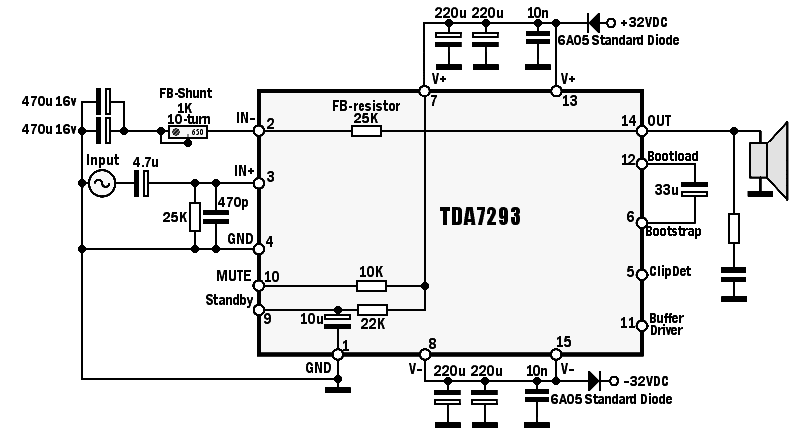
A quick fix for that schematic at Post#539 would be: Change C2, C6 & C7 all to high quality 470uF caps. Or, if board space permits, change C2, C6 & C7 all to 440uF (ordinary 220uF caps used tandem for 440uF at all three locales).
P.S.
That schematic at Post#539 (and in the datasheet) is incomplete and therefore please see the Stability chapter in the LM1875 datasheet.
Hi Daniel, I want to built a stereo system using your schematic LM1875 turbo II to drive a pair of 4" 6 ohm speakers
I currently own a 3A transformer center tapped with 12, 18, 25 and 32 volt, my question is whats your suggestion for me in choosing those available secondaries to achieve its best performance?
and one more thing, what happens if I replace the input caps from 2u2 to 1u?
what are the advantages / disadvantages? should it use a non-polar ? and why?
please enlighten me
thanks
__________________
iwan
18VAC should be good. It gives about 24V DC.
25VAC is too much as it gives about 34V DC and sheet suggests +-30V max.
25VAC is too much as it gives about 34V DC and sheet suggests +-30V max.
For fake/clone chip use the 12v option and slightly lower gain.Hi Daniel, I want to built a stereo system using your schematic LM1875 turbo II to drive a pair of 4" 6 ohm speakers
I currently own a 3A transformer center tapped with 12, 18, 25 and 32 volt, my question is whats your suggestion for me in choosing those available secondaries to achieve its best performance?
With real LM1875, you can use the 18v option--that and fuses too.
1uF is fine for input cap. You'll have cleaner sound that way. There'll be slightly less bass but also less boomy/warm bass noise as well. Polar or non-polar are both fine for this use.and one more thing, what happens if I replace the input caps from 2u2 to 1u?
what are the advantages / disadvantages? should it use a non-polar ? and why?
please enlighten me
thanks
__________________
iwan

No,
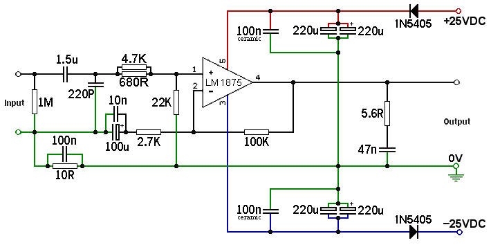
1M||10k||220pF
I'm not sure what the 47k is doing. Is it creating output offset?
1M||10k||220pF
I'm not sure what the 47k is doing. Is it creating output offset?
Last edited:
The Loop AREAS of the inputs (+IN & -IN) are enormous. Not good for interference attenuation.
Last edited:
So the input impedance is about 9kOhms, because impedance of the capacitor is variable depending on the frequency, right?
47k and 1k5 is a voltage divider for NFB.
And about loop areas. So the +In would be better like that (rough example):
47k and 1k5 is a voltage divider for NFB.
And about loop areas. So the +In would be better like that (rough example):
An externally hosted image should be here but it was not working when we last tested it.
the loop AREAs are still enormous.
The 47k is creating an output offset because the +IN & -IN resistances are very different.
The 47k is creating an output offset because the +IN & -IN resistances are very different.
Worst case 2uA input bias current means about 80mV offset. Typical 200nA input bias current means 8mV offset. Maybe some chips will have significant offset.
One solution would be to solder a 8.2k resistor from the right pin of the 47k to the left pin of the 1.5k, and use about 2200uF for the 330u cap.
One solution would be to solder a 8.2k resistor from the right pin of the 47k to the left pin of the 1.5k, and use about 2200uF for the 330u cap.
Last edited:
That is the size of half a business card. The size could be halved again if SMD parts are used to make it smaller than a stamp, such as approximately coin size. Smaller loop area is doable at the cost of having no space for a standard soldering tip to fit.the loop AREAs are still enormous.
Output offset is 3mv~45mv depending on chip manufacturing variance. One may note that a tight input load Reduces output offset. When you're looking at skewed resistor values, then you're looking at a chip amp Rigged to run at slightly higher voltage than it should. It was either that or derate for 40% less output power. That's not a big concern for a TDA7293 because either 70W or even 45W is far too loud inside a normal house. However, cutting off 40% of LM1875's output power might be of greater concern due to clipping distortion--I assumed that was a far too high price to pay for parts value monotony.The 47k is creating an output offset because the +IN & -IN resistances are very different.
Although not assumed to apply for non-inverting amplifiers, a different possibility is that you could be looking at where a buffer should have been used and wasn't.
CM-rejection style input, rarely seen on buffers, never on audio amplifiers, is one of the very few times that symmetrical resistor values are useful. Usually it is more important to balance out the current instead. However, albeit horrendous labor, it is entirely possible to do both at once on an audio amplifier, without adding any more active devices.
So thank you!
Therefore, I suppose that the future plan is to combine the newest power circuits with a novel balanced current AND CM-rejection style input circuit for the proposed 2016 editions.
I do happen to have balanced current design, using symmetrical resistor values, 25k for input load, 25k for feedback, in the form of the latest 45W TDA7293 Solo. It is compatible with CM-Rejection style of input circuit (no matter that it should be put on a buffer, not an amplifier). However, those features have not yet been combined.
I don't have a balanced current LM1875 yet; however, I do have a proposed rough draft for one with both the skewed resistor values and CM-Rejection style input:
(this is the LM1875TurboII with the CM rejection feature hastily pasted on, rather than thoroughly incorporated--the combination is not tested)
Notes:
See the identical voltage divider proportions.
Un-skewing the resistor values, to make the input load value same as the feedback resistor value could be done via derating and is expected to cost most of the output power, although that is certainly doable--operating voltage would be no higher than +-18vdc, and it is after that change when matching up the resistor values will work just fine.
Last edited:
The sch in post552 is wrong.
The input components are in the wrong places.
nearly as indecipherable as
The input components are in the wrong places.
what does that mean?Un-skewing the resistor values, to make the input load value same as the feedback resistor value could be done via derating and is expected to cost most of the output power,
nearly as indecipherable as
When you're looking at skewed resistor values, then you're looking at a chip amp Rigged to run at slightly higher voltage than it should. It was either that or derate for 40% less output power.
Another go at saying the same thing: Significant derating (especially "under-volting") can improve the linearity to the point where orthodox component values have also become optimal component values. I think that is a linearity matter.
Matching up the voltage is probably important, and need not involve actually matching the resistor values.
For example:
Feedback 50k, feedback-shunt 1.5k
Input load 25k, in+series 750R
Those two voltage dividers are the same proportion and thus the voltage situation does match up just fine.
In that example, the 25k is pushed by a little source device; however, the 50k is pushed by an amplifier (and there's gain on it too). That difference is insignificant for buffers (no gain) and also insignificant for power amplifiers run so lightly that the linearity tolerances are forgiving.
Those exact values are non-specific and for discussion purposes--actual values require at least two days of proofing, possibly faulted by two guesses: The exact speaker load and the average output power needed. The matter is current, and the current demand cannot be the same for everyone. For sure, the current from a source or from an audio amplifier, will be different.
The datasheet example schematic can do an acceptable job at up to 11 watts output power. Had you wanted more, then a compensation may be needed for practical audio quality.
#552
Daniel, you should reference the opamp inputs to a single point. The 10R separating the two will only increases THD.
I don't understand your matching of resistors, as it seems to me that even 1k - 20k does not match 20k - 1k as a voltage divider.
If you are looking to have the same current for each voltage divider then the feedback resistors should be X time larger than the input resistors, where X is the gain.
Example: Gain=21, input 1k-20k and feedback 21k-420k.
Does this make sense? Not very practical I think.
Thanks for catching that! That schematic was made for the purpose of asking a question. And that question is input noise rejection, like this:#552 Daniel, you should reference the opamp inputs to a single point. The 10R separating the two will only increases THD.
Common mode rejection by BV
Looks like a buffer should be doing that job, because an amp will be less effective by proportion of the gain (so that won't be perfect); however, it still wouldn't miss by much.
It seems that the limiting factor is the power voltage, not the gain. Assume a range of 10k~114k could be used for feedback resistor, and that range also represents minimum and maximum power voltage. That'll land within a few miles of the ballpark. One may still have to resort to trying the whole range of resistor values one at a time. I wish there was an easier way....If you are looking to have the same current for each voltage divider then the feedback resistors should be X time larger than the input resistors, where X is the gain.
Example: Gain=21, input 1k-20k and feedback 21k-420k.
Does this make sense? Not very practical I think.
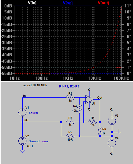
Yes, the ground loop voltage is over R5, that is in series with R4 (and R2).
Moving R4 to the input ground (SG) will lower the signal at the output.
Moving R4 to the input ground (SG) will lower the signal at the output.
Last edited:
Sorry. I can't quite imagine how to improve on that unless the critiques are in schematic form.
- Home
- Amplifiers
- Chip Amps
- Beginner's Gainclone, HiFi LM1875, The Amplifier Board