My PL X2.5 preamp cannot drive this beast. The output impedance of my X2.5 measures ~190 ohms.
You have a short somewhere.
The DC leakage current is nanoscopic.
The input capacitance of about 120 devices is about 4,000pFd, which is about 2k Ohms at 20kHz (so -1dB), 40k at 1kHz (-0.05dB).
NP configures a driver (from one of the cells) to drive a certain number of the cells, in his Beast.
Does anyone know what the Cgs is for a cell?
Also, how many cells are you running for 1Amp Bias?
Since there is no voltage gain, Mr. Miller isn't making an appearance, at least.
I set up a measurement of capacitance of one cell. There is a 1k resistor in series with every cell input. I measured the voltage across one of these these resistors at 10kHz at 11.4 v p-p input. The AC voltage across this 1k resistor is 10.2 mV.
My calculation is that the input capacitance is 40 pf which would make the entire PCB 3.2 nF. There are 80 cells on this PCB.
There is a 1k resistor from PCB input to ground at the moment.
Does anyone know what the Cgs is for a cell?
Also, how many cells are you running for 1Amp Bias?
Since there is no voltage gain, Mr. Miller isn't making an appearance, at least.
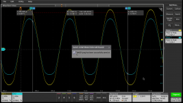
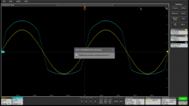
Attached scope capture, yellow trace is input from sig gen to PCB at 1kHz. Blue trace is output from PCB to 3.3 ohm power resistor.
Not too bad for a handful of gnarly JFETs.
Attachments
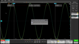
Same setup 8 ohm load. 4.7 watts RMS into 8 ohms. My sig gen stops at 20v p-p. You can get more power with higher voltage rails and/or more drive voltage. I would run this PCB at + / - 15 if you want absolutely the most output.
Looks beautiful. Do not use this amp with a 3.3 ohm speaker.
Looks beautiful. Do not use this amp with a 3.3 ohm speaker.
Attachments
To offset grid leakage, probably 12-18k to neg rail will be better.There is a 1k resistor from PCB input to ground at the moment.
To offset grid leakage, probably 12-18k to neg rail will be better.
Thanks. I will give that a try.
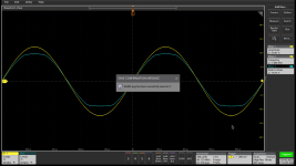
It looks to me like the negative going 1/2 runs out of current first. I think that this is a symptom of the need for a larger source resistor of the P JFET to balance Idss of the N JFET.
Oops, wrong magnitude, should be 12-18M hence impractical. Sorry.
No worries. I appreciate the discussion. If you look at the scope shots above, this amp works well until you hit current clipping and it clips softly. I think a good low impedance driver is all that is needed to make this amp a complete package.
No need for heat sink and the temp coefficient is self-stabilizing. If you build 4 PCBs and run balanced, you can easily get 10-20 watts. It is just not high current and low impedance.
Being a complementary power JFET output stage, it is very unique.
I have a single ended version PCB in-hand. Look back in the thread for the single ended version.
Was it the layout in post #208 that you got fabbed?
Beast with 1000 JFETs redux ?
No I have not laid out a cascode single ended buffer PCB. In post 213, Mr. Pass gave his opinion on how the cascode single ended buffer might work. It is on my list to do. I have not shared any of the layouts; just the basic cell. The PCB is 99% step and repeat of the basic cell.
The PCB that I am working on now is a complementary buffer similar to the the original Beast. The PCB is shown in post 225 of this thread. The PCB is labeled as complementary. The basic cell is shown in this thread.
I also have a PCB of a single ended version but it is not cascoded. My version is similar to the version Mr. Pass made (shown in post 131 of this thread).
Last edited:
80 cells will yield over 1A idle current per PCB.
Thought my little OTL headphone amp was naughty.. 100mA 200V idle class A, or 240mA max, per channel. Toasty. That has 4 parallel triodes on each output.
How do you drive that without any frequency rolloff etc?
Thought my little OTL headphone amp was naughty.. 100mA 200V idle class A, or 240mA max, per channel. Toasty. That has 4 parallel triodes on each output.
How do you drive that without any frequency rolloff etc?
At the moment, I am driving it with a small power amp. This is just for the purpose of taking measurements.
In practice, I will drive it with a DIY low impedance buffer. Working on that now.
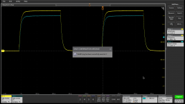
Any " Beast " square wave input and output shape test ? 😀
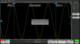
Yellow input to Beast. Blue output from Beast to 8 ohm load.
Attachments
No I have not laid out a cascode single ended buffer PCB. In post 213, Mr. Pass gave his opinion on how the cascode single ended buffer might work. It is on my list to do. I have not shared any of the layouts; just the basic cell. The PCB is 99% step and repeat of the basic cell.
The PCB that I am working on now is a complementary buffer similar to the the original Beast. The PCB is shown in post 225 of this thread. The PCB is labeled as complementary. The basic cell is shown in this thread.
I also have a PCB of a single ended version but it is not cascoded. My version is similar to the version Mr. Pass made (shown in post 131 of this thread).
Thanks, I did mean layout of cell rather than PCB.
Very interesting work.
Cheers
- Home
- Amplifiers
- Pass Labs
- Beast with 1000 JFETs redux?