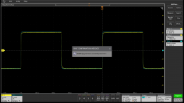
Yellow input to Beast. Blue output from Beast to 8 ohm load.
Input yellow wave form is less square than normal, probably need use calibrated probes ?
Have a nice day 🙂
Input yellow wave form is less square than normal, probably need use calibrated probes ?
Have a nice day 🙂
Probes are properly compensated. Input capacitance of amp is 20nF measured. Sig gen output impedance is 50 ohms. -3dB freq is 160 kHz. That is why the rounded leading edge of square wave.
If driving buffer output impedance is 10 ohms, -3dB freq rises to 800 kHz.
If you like square waves, you need a very low impedance driver with low input capacitance.
RC Filter calculator (Sample)RC Low-pass Filter Design Tool - Result -
..One cell populated J113 (D-S-G) with 33 ohm source resistor and J175 (D-G-S) with 47 ohm source resistor..
I was reading through some old related threads and wonder if using J176 instead of J175 would be better for this application?
how about using J111 J175 Jfets in F5
If you are interested in complementary pairs for followers or as CFA
input stages, my preferred parts are the 2SK170, 2SJ74 (or the Linear
Systems equivalents). but the J113 and J176 are good enough for most
of these circuits.
What about using a j175 with 1mA more idss than the j113 and degenerating it with 10r resistor?
I think you will find the J176 to be a better match to the J113. Push-pull
degenerated down to 10mA bias, I get about .016% thd driving 10 Kohm
at 1 volt.
The attached spreadsheet is from post #197 of this thread. You can see that the J175 roughly matches the upper half of the J113 distribution while the J176 roughly matches the lower half of the J113 distribution.
It is the builder's choice how to populate the PCB.
I have thought of using a mix of J175 and J176 to match the J113 population while I was building this first board. Up to now I have only used J175.
Last edited:
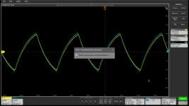
Square wave as requested. Input to the power amp overlaid with output from the power amp. No load condition.
This measurement required me to dig up a preamp that I worked on a few years ago.
VSSA as preamp/driver
This measurement required me to dig up a preamp that I worked on a few years ago.
VSSA as preamp/driver
Attachments

With these new measurements, the output impedance of the power amp calculates to be ~ 0.95 ohms.
Looks good 🙂
I agree. Single stage power JFET amplifier with no overall negative feedback. No surprise that it looks good on the square wave test.
The preamp I am using is quite impressive. It can do 64v p-p before clipping. It is the BJT equivalent of a BA3 preamp but with + /- 33v rails. This leads me to want to lay out the cascoded Sony VFET front end using + / - 35v rails. A poor man's wanna-be XP30.
If you have access to a scope and a sig gen, you can test if your beast is causing your preamp to slew.
That is a slow rise time, at least compared to what the input frequency needs to reach the positive level.
The part of the waveform shown will remain the same shape as the frequency is lowered.
Slew rate limiting would show a more linear rise. like this:
Attachments
That is a slow rise time, at least compared to what the input frequency needs to reach the positive level.
The part of the waveform shown will remain the same shape as the frequency is lowered.
Slew rate limiting would show a more linear rise. like this:
The capacitance is likely non-linear; maybe very non-linear. I would have to measure it to know for sure.
If that were the case, the shape of the output would vary with the input level.
It does. The scope trace in post 290 is a logarithmic approximation of a triangle. It leads me to postulate that the input capacitance is rising with voltage in a logarithmic manner. It looks like the slew rate is decreasing with increasing voltage.
Try a triangle or sawtooth, much easier to visualize than changes to the 1 - e^(-t/RC) rise.
Last edited:
Any updates on this cool project?
The first fully populated board is up and running at 1A idle current.
The input capacitance is so high that I believe most DIY users will not be able to drive it and achieve lowest slewing problems.
Either I design an external driver or re-lout the board with an optional driver stage. This is exactly what Mr. Pass did. Now I see why.
I have boards that are perfectly usable if you can drive it. If there is interest, I can open a group buy thread in that forum. I will wait to do a full build until I layout the buffer version.
There are exactly 8 of these PCBs available.
New layout is hopefully finished. The top row (8 cells) is the input stage. The bottom 9 rows are the output stage. 6 PCB layers; Input, Output, GND, V+, V- and IntermediateOutput. The intermediateOutput layer is the output of 8 cells that comprise the first stage.
In the previous layout, there was a redundant layer as there were only 5 nodes in the circuit. In this circuit, there are 6 nodes and there is no redundant layer.
An input resistor to ground has been added. There is a resistor from IntermediateOutput to ground.
There are silk screen labels and arrows for probing the InermediateOutput node.
Attachments

- Home
- Amplifiers
- Pass Labs
- Beast with 1000 JFETs redux?