Hello Andy,
I also use those testclamps that ItsAllInMyHead suggested in his post #492.
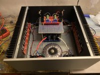
The distance from the resistorlegs (R10/R11) to the small heatsinks of the MosFets is very close! 😱
What a pitty! I feel with you 🙄
Don't give up!!!! Looks like you are walking through the 'valley of pain'?
Greets
Dirk
Perhaps time for a beer or a wine?
This is totally my own fault. So I cannot let it stop me. I have to prove I can make it. My fault was being impatient while biasing, moving probes without turning off the amp. So you might regard me somewhat of an idiot. Perhaps I am, but all actions were taken in the spirit of music.
Don't beat yourself up over this; chalk it up as a learning lesson.
The damage isn't too bad. So a couple resistors and perhaps the mosfets.
Unless you're using NOS Toshiba mosfets, everything is easily replaceable.
The damage isn't too bad. So a couple resistors and perhaps the mosfets.
Unless you're using NOS Toshiba mosfets, everything is easily replaceable.
Thats about my assessment as well, resistors of course need replacement, and perhaps MOSFETs. What do you think my changes are with the MOSFETs? They are Fairchild, so easy to source and actually allready on the way. But I am rather concerned I’ll destroy the solderpads replacing them. They are the smallest pads I have seen on the Pass boards I have. Which, btw, arent to many. But none of the F5T pads are that small. Luckily a new board is on the way. But I did put a lot of effort into this FE board, so I hope it survives.
Last edited:
Fixing this thing, and testing it: If I use a lab supply with variable DC, how many amps do I want to expose the FE for? The one I am looking at, is rated from 0-5 amps, adjustable.

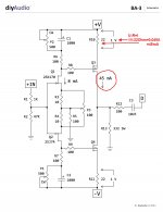
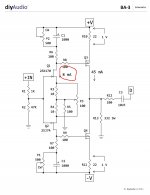
Yep, I agree with Denis. The rest of the circuit is also 'sucking'. The JFets also want to 'eat' a little bit - although only a few mA.
For both channels on the BA-3 FE-board around 100mA.
Greets
Dirk
Thanks.
I will only be powering up one channel at a time. Till give it around 50 ma, and hope all goes well.
Correction: 45ma per device=90. So give it 95 perhaps? No light bulb tester so far, but planning to get a cheap variable lab supply that will enable me to test all boards prooperly, except PSU board. But that works fine.
Last edited:
Ok, so teturning to the circuit obviously has its advantages.
8ma X 2 = 16
45ma X 2 = 90
So setting the lab supply to 110-120ma for starters, seems like an OK plan?
8ma X 2 = 16
45ma X 2 = 90
So setting the lab supply to 110-120ma for starters, seems like an OK plan?
two outputs are connected in series, practically same as everything is in series (looking from one rail to second), current flowing from one rail to other
in short - current through one JFet is same current flowing through second JFet
also - current through one Mosfet is same current flowing through second Mosfet
............
it'll be then (speaking of one channel ), to paraphrase you :
8ma X 1 = 8
45ma X 1 = 45
in short - current through one JFet is same current flowing through second JFet
also - current through one Mosfet is same current flowing through second Mosfet
............
it'll be then (speaking of one channel ), to paraphrase you :
8ma X 1 = 8
45ma X 1 = 45
If you are apprehensive... You don't need to fully bias Q3 and Q4 with the lab supply in place.
If you've set P1 and P2 back to their zero points (which I'd recommend) and have P3 back to the middle - then you won't need full current. You can always try a lower amperage limit at first just to test other parts of the circuit before biasing Q3 and Q4.
tl;dr - you can start at ~20-30mA to check everything but current flow through the Q3/Q4. You could check around your JFETs (Q1/Q2) etc. You could even start to get a bit of current through the MOSFETs by checking P1/P2.
Then, once you know everything is looking good, you can bump up the current and make sure it begins to bias properly. After that, you can use your new shiny dim bulb tester, if you decide to build one, to hook it to your PSU for one last check.
Those are my initial thoughts after making an attempt to study the schematic one more time. Someone with expert knowledge can confirm if that's a safe path and if the JFET section of the circuit would provide proper readings w/o the MOSFETs conducting. I think it should based on the startup process and other things from Papa's article, but best to have someone else chime in just for safety.
Edit - ZM's on.... Listen to him... 😀
Last edited:
Thanks guys. Enlightening. I will start low, and gradually increase, and see what happens. Parts arrive tomorrow, but uncertain when I will have time to get back to «work». I will re-read Nelsons manual, plan my test, and maybe check in with you guys before getting to work. Really, thanks!
Checked the other channel today, and as expected it behaves as it should.
Btw I ordered new tesprobes off amazon. The ones linked a few posts above, as well as some small enough to be used on SMD. Bith types will probably do the trick, but given the extra costs involved in overseas shipping and customs, I ordered both types. Thanks for the tips, guys!
Been thinking about max bias and the question of overall dissipation.
The BA-2 output boards 6 deep dissipates around 300 watts, according to Nelsons BA-2 article. I wonder how this figure is calculated. 6 watts per device, times 24, equals 144. Not around 300. So either we are talking about different types of wattages: disspation VS bias, or for some physics reason the number 144 must be multiplied with 2, giving overall dissipation. Times 2, that is 288. This also explains why a transformer of 600va is the minimum requirement.
Can someone shed some light on how this works?
One of the reasons I ask is I run 3 deep, and bias the MOSFETs to 12 watts per device. This gives the same overall figures as 6 deep 6 watts per device. I THINK I have some headroom wrt temperature (but have to let it cook for longer to know for sure), but if the rule of total watts times 2 applies, max wattage per device in my case will be 12,5 watts as my transformer is «only» 600va.
Regards
Andy
- Home
- Amplifiers
- Pass Labs
- BA-3 Amplifier illustrated build guide