Sure, but a CFB stage biased in class A is not the optimum overall.
It really matters on the listening volume and the speakers, how efficient they are.
As far as i know there is no listening test published about bias in a CFB stage.
Some voluntaries ?
It really matters on the listening volume and the speakers, how efficient they are.
As far as i know there is no listening test published about bias in a CFB stage.
Some voluntaries ?

hehe... nevertheless the nobrainer works quite well 🙂
🙂 That's how it goes, we do not expect to build the 'final answer to OPS, VAS and INP' in one go. That needs a bit more work. The intermediate results are needed to learn from and to evaluate. Choices are wrong or good, that does not matter as long as we try for excellence and bring each experiment to a conclusive (note: not successful) end, we are doing good.
https://www.youtube.com/watch?feature=player_detailpage&v=aboZctrHfK8
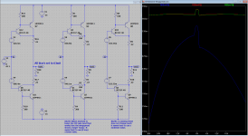
While waiting for the boards I have been playing with simulations using MJL3281 and MJL1302 for the output..... needed to reset the vbias value and it sims ok but somehow it looks much more sensitive to miller cap and distortion also higher when input is over 1v.
Attachments
Frans, when you lower the internal gain in the way you are doing you should put the 0.22 resistors in the emitters of the power transistors not in the collector , and you have to lower the emitter and collector resistors of the driver transistors , use 22 ohms for both like Ricardo is using.
I think what Frans wanted to show is that R6, R7 are too big in my original design.
I copied that simply from JLH.
Maybe he put them there to make the amp more stable.
In later designs he abandoned them.
I copied that simply from JLH.
Maybe he put them there to make the amp more stable.
In later designs he abandoned them.
Frans, when you lower the internal gain in the way you are doing you should put the 0.22 resistors in the emitters of the power transistors not in the collector , and you have to lower the emitter and collector resistors of the driver transistors , use 22 ohms for both like Ricardo is using.
Sergio, yes I know, but this is not what I am using, it was done to show the effect of these in simulation, and to provoke discussion (as is working). I'm not building this, or the JG amp, I'm just poking a bit and helping to keep the ideas going. As I just discussed this with Joachim, I noted that it would be a good idea if other people put there idea's in simulations and show us there results, so... make it so 🙂
https://www.youtube.com/watch?feature=player_detailpage&v=X6oUz1v17Uo
Yes, better thermal stability is the advantage of CFB output stages.
Plus less idle for " optimum THD " then a simple EF stage.
Plus less idle for " optimum THD " then a simple EF stage.
Well, they just take apart the CFB on the othere thread, poor Ricardo.
Hope that this will clear things a bit 🙂.
The output stage that Ricardo uses is not a CFP stage, it does not have the high internal gain that CFP stages have, it does not have the same thermal feedback that a CFP stage have, it does not behave like a CFP in the crossover point.
It resembles much more with a EF stage but with even less gain than a EF stage, all the comments about CFP stages that was made in the Douglas Self thread are true, but they not fit in here.
I think what Frans wanted to show is that R6, R7 are too big in my original design.
I copied that simply from JLH.
Maybe he put them there to make the amp more stable.
In later designs he abandoned them.
Ok , I was out of context. Sorry Frans.
While waiting for the boards I have been playing with simulations using MJL3281 and MJL1302 for the output..... needed to reset the vbias value and it sims ok but somehow it looks much more sensitive to miller cap and distortion also higher when input is over 1v.
Ricardo, there are some problems that you need to address in your design. The most important is that you can not use the BC327/337 in those positions you have to use bjt with at least 80Vce, the 2sc2240 will work but have different pin position than the bc327/337.
Other is that the open loop phase margin is only 40º, that is due to the R30, R31, you need to shunt this resistors with a capacitor (at least 100n)
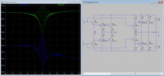
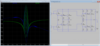
This is the EF vs Ricardo output stage (ROS for short 🙂 ).
The second image the emitter resistors of the EF have to be increase to 0.6 for matching the ROS gain, the ROS have a lower gain than the EF because is driven by a higher impedance , in terms of thermal control I think that ROS and EF may be very similar, the ROS may be more thermal stable and emitter resistors can be even lower than 0.2 for lower crossover distortion, I think that even a 0.1R will work here, but is need further testing.
Like the EF stage, in ROS also all the output, drivers and bias spreader transistors must be mounting in the same heat-sink for thermal control ..
Attachments
Last edited:
- Home
- Amplifiers
- Solid State
- Assemblage Power Amp