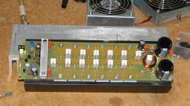
Very impressive Anthony. Is the little board the phase inverter? What rails does it run? Is the heatsink big enough?
Very nice PCB (space saving layout).
Cheers
Very nice PCB (space saving layout).
Cheers
Thanks Quasi
The little PCB is a voltage regulator board +-15 volts
to run the opamps, voltage translation stages and the cold amp first driver stage.
The the hot and cold sides of the output stage runs on a single supply rail of around 150 volts.
The heat sink is a Conrad MF35-151.5.
Its big enough for home use. But for Pro-audio use forced cooling would be a good idea.
The PCB is double sided PTH and I have used SMD components in the driver stages.
I have got a bit more work to do on the PCB to add more SMD devices and put the Filter caps on the PCB instead of handwired as you see them here.
Hi Anthony
Dan is running +/- 93 volt rails with around 1kVA of power supply per channel. Allowing for say 10% total losses he should get around 420 watts into 8 ohms and maybe 700 into 4 ohms. FETS are IRFP460. Dan tells me he'll be doing a power test soon.
Cheers
Q
Dan is running +/- 93 volt rails with around 1kVA of power supply per channel. Allowing for say 10% total losses he should get around 420 watts into 8 ohms and maybe 700 into 4 ohms. FETS are IRFP460. Dan tells me he'll be doing a power test soon.
Cheers
Q
Dan,
can you arrange for a -20db flick switch on the test signal to your amplifier?
Set up the amp and test load and DVMs and oscilloscope.
Set flick switch to -20db.
Increase input signal to give 10% of expected maximum signal.
Reset oscilloscope sensitivity to suit the next stage.
Flick the switch to 0db and quickly check the scope for clipping and immediately flick back to -20db.
This keeps the sink and output stage and test load at a low temperature and you give the test temps time to recover.
Adjust the -20db test signal and briefly repeat the high power test until the signal is just below visible clipping.
repeat and take an output voltage reading. Job done @ 1kHz and hopefully no over temp blow ups.
Can you check the accuracy of your DVM @ 1kHz?
If your input signal is just a few percent high and causes the output to just clip, you can observe in that one second or so the clip developing as the PSU voltage sags.
This procedure avoids the need to gate the test signal and gate the observation signals to prevent massive temp rises in the load and output stage.
whoops anthony, my email took me to the last unread post...
150V rail, = power 🙂
Thanks for the extra fet the one i sacrificed in haste was the only one i popped (phew)
😎
the second channel is now up and running 😀
now i just have to finish the case and i am ready to some speakers.
Thanks Quasi!!!
-Dan
150V rail, = power 🙂
Thanks for the extra fet the one i sacrificed in haste was the only one i popped (phew)
😎
the second channel is now up and running 😀
now i just have to finish the case and i am ready to
some speakers.Thanks Quasi!!!
-Dan
Hi AndrewT,
In response to your question(s)
-my "sig gen" can easily be set for 0-20db
-I can check the accuracy of my DVM @ 1kHz
-Typically i am only testing to see what the max voltage at a given load is and then calculating power from this.
-I prefer to start at 0V input and slowly increase the input signal watching the scope until amplifier clipping or power supply limiting occurs.
-Typically during testing i only check maximum output power for a short period of time (less than 30s)
-Dan
That slow process of gradually increasing towards maximum power is exactly what will kill your amplifier and/or your load.danieljw said:-I prefer to start at 0V input and slowly increase the input signal watching the scope until amplifier clipping or power supply limiting occurs.
-Typically during testing i only check maximum output power for a short period of time (less than 30s)
That's why I asked if you can arrange a -20db flick switch.
30 seconds ?
.
That might be too long Dan. I generally look at max power for only about 10 seconds.
So now you have two working modules, cool. Have you told the neighbours?
.
That might be too long Dan. I generally look at max power for only about 10 seconds.
So now you have two working modules, cool. Have you told the neighbours?
Hi Dan and Quasi
Have you looked at the thermal compensation closely on this module.
How does it behave?
Does it over compensate or under compensate?
Ideally you should be able to measure a stable bias current at idle which it would have.
But at full power it should remain fairly constant.
I have done quite a lot of work in this area.
I have a version of my NX500NL working with 8 x IRFP260N devices.
With the module running at full power which is around the 800 watt level.
The bias remains constant. It took a lot of development to make this work correctly.
With this in place the amplifier is able to sustain full power for hours on end.
The simple Vbe multiplier used in most amplifiers just does not work right.
In this case they would under compensate with these devices.
Thermal compensation
.
The thermal compensation in this design is very simple and provides only satisfactory results.
During the amps warm up phase it tends to over-bias a little and then backs off as the amp reaches it's normal operating temperature. During heavy use the bias backs off further, probably too much, and climbs back up as the temperature drops.
So the bias setup for this amp module requires extra care, and must be observed, as Dan has found, over a longer period before it is finally set.
With this schematic I have found that the biasing is controlled best if the sensing transistor (diode) is placed as close as possible to the FETs.
No doubt you've picked this shortcoming instantly. Whilst I do not want to change the set-up too much I would be grateful for any ideas you're able to share.
In my other amp "Power Amp under Development", the bias using the sensing transistor I've chosen moves by only a few %. This will depend though on the constructors choice of layout.
Cheers
Hi Quasi
While the bias arrangement works well on my amplifier.
For yours it may require some tweaks.
Which amplifier schematic is dan using?
What I found was it is a balancing act between the number of output devices used/Supply voltage used/Source resistor value.
Also at least a couple of MJE340 devices wired as diodes where inserted in series with the bias pot of the Vbe multipiler, or in this case with my amplifier Vgs Multiplier.
Also the Vgs device and the MJE340 devices where mounted directly on top of several output devices.
With any of these Vfet devices such as the IRFP450 or the IRFP260N, in general as voltage supply is increased they become increasing more difficult to thermally stablize.
+-60 volts and below is very easy to stablise these devices, above +-70 volts it becomes very interesting.
I have seen for instance Greg Balls SKA amplifier schematic actual GB300.
This amplifier would suffer the same problem, hence why I believe he only runs his amplifiers no higher than +-75 volts.
and can only get no more than 300 watts from his designs.
Don't get me wrong I am not having a go at Greg, I have meet him in person in Qld and we spend a day together at an Audio club meeting.
Just proving a point I guess.
Anyway I hope this helps you improve your thermal management
on your amp.
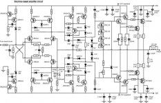
Hi Anthony,
This is the schematic that Dan has used. http://www.diyaudio.com/forums/attachment.php?s=&postid=991050&stamp=1156601436
As you can see the thermal compensation approach is quite different. In this circuit, thermal compensation is achieved by varying the second stage constant current source. As T4 (mounted in the heatsink) heats up its Vce drops robbing base drive from T5 and this backs off the current in the second stage. The FET Vgs drops and the bias falls away. Simple and effective enough, but not as constant as the normal Vbe (Vgs) arrangement.
I too have placed the heat sensing device directly on the FET before, but with this layout with the FETs under the PCB, it's not possible.
Please take the time to have a look. I would value suggestions you have to improve the situation.
Cheers
Quasi
Hi Quasi, Hi Saint, Hi AndrewT
Quasi -
I have not informed the neighbours........ they will know dont worry 😀
Anthony-
there is a schematic floating around with a similar thermal comp cicuit to what you mentioned (mje340s wired as diodes) it looks like an interesting concept keep up the good work.
AndrewT-
I do realise why u specify this method, and thanks for the advice.
I might give a try and let you know the results.
-Dan
Hi Dan and Quasi
Thanks Dan I will endevour to improve all the time.
Quasi your biasing arrangemnt is over compensating.
The first area I would try is to drop the value of your source resistors down to 0.22 Ohms.
Before you do that you might want to replace D5 with a 1n400x
The junction on the 1n4148 is likely to drift more with ambient temp. also I would try putting an extra diode in series with D5 and T4. This should I think reduce the over compensation issue.
Give it a try anyway and keep me informed.
Also Dan where is that schematic you mentioned, I wouldn't mind having a look at it.
Hello Anthony
How about no Thermal compensation!!!!
I dont have any type of thermal compensation in my NVMOS amps with the rails +-150VDC idle......with the bias current 25mA per Mosfet.......😉
best regards
Kanwar
How about no Thermal compensation!!!!
I dont have any type of thermal compensation in my NVMOS amps with the rails +-150VDC idle......with the bias current 25mA per Mosfet.......😉
best regards
Kanwar
- Status
- Not open for further replies.
- Home
- Amplifiers
- Solid State
- Another quasi-complementary design