Thanks to both of you. After resetting the P1 and P2 I have turned the amp on and it seems to be working well. I'm so relieved I didn't fry any components. I am measuring about 570 mV across R7 and R8 and just a few mV across the speaker terminals. I'm going to let it cook for a while before installing the other board but so far so good.
I've read different things about the optimal voltage across R11 and R12 to target. Is there some agreed upon value for best sound quality or is it simply driven by the temperature of the heatsinks? Right now the Mosfets only measure 35 degrees C but they have also only been on for 10-15 minutes.
I've read different things about the optimal voltage across R11 and R12 to target. Is there some agreed upon value for best sound quality or is it simply driven by the temperature of the heatsinks? Right now the Mosfets only measure 35 degrees C but they have also only been on for 10-15 minutes.
Paul,
It sounds like you've adjusted P1 and P2 to bias up the output stage. Can you please
confirm that you removed the bulb tester before you started the bias procedure?
If you've turned up P1 and P2 (and getting 570mV across R7 and R8) with the
bulb tester still in place then I'm afraid you need to turn P1 and P2 back down ,
remove the bulb tester and start the bias procedure again.
The original F5 spec'ed the bias as 0.6V across the 0.47ohm source resistors
(R7 and R8 in the current schematics and PCB) so I would suggest just going with
that for now.
I did remember to remove the dim bulb tester before biasing. I'll wire up the second board tonight. Fingers crossed I don't make the same mistakes twice!
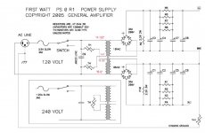
How should the PSU ground be wired? Should the ground from each rail only connect at one point at the final capacitor on each side like is shown in the F5 PSU schematic--although its ambiguous. Or should there be a ground bus with the ground side of all 10 capacitors in the PSU connected to it? And should the ground of each bridge rectifier be connected together as well?
Attachments
Can you post photos (top and bottom) of your PS board? Or maybe you haven't started yet.
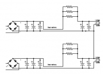
These are two identical (except for the location of the resistors) floating power supplies.
They are connected together only at their output terminals, one positive and one negative,
to make a +/- supply.
The connections within each supply should be arranged keep the rectifier charging current pulses
confined to the first two capacitors, and out of the other connections in the supply.
Last edited:
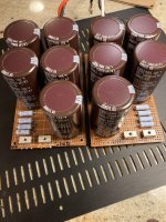
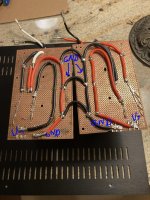
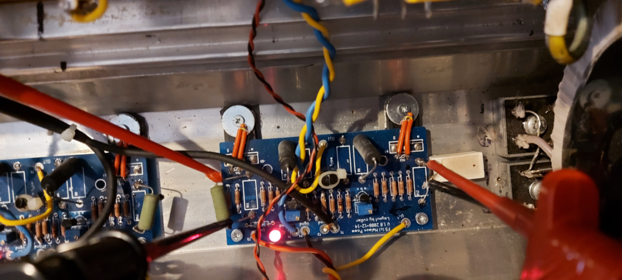
rayma, here are photos of my power supply I made.
From what you said, I think I should not have the grounds of the last 3 capacitors of each rail connected together. Only the ground of the last 1 and that should be the location where I connect the amp boards ground as well. Is that correct?
From what you said, I think I should not have the grounds of the last 3 capacitors of each rail connected together. Only the ground of the last 1 and that should be the location where I connect the amp boards ground as well. Is that correct?
Attachments
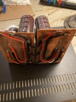
The idea is to have the rectifier and input caps all in one circuit, and then bring out, directly from
the cap terminals, the two +/- leads that go to the output resistors/capacitors.
This keeps the current pulses away from the output terminals of the PS.
There should be only one connection between the two supplies, located right at the output terminals.
Do you have 3 caps for the input section, and 2 caps for the output section, or the reverse?
I'll draw up the routing arrangement for you later today.
Last edited:
Like this, two sections joined by two wires. Jumper between them at the outputs.
You may have the group of three capacitors at the outputs, instead of the inputs.
The resistors (you may have four of them) can also be on the bottom wire
in the lower supply, as per the Pass schematic. It was just easier to draw it this way.
You may have the group of three capacitors at the outputs, instead of the inputs.
The resistors (you may have four of them) can also be on the bottom wire
in the lower supply, as per the Pass schematic. It was just easier to draw it this way.
Attachments
Last edited:
Ok cool I understand that. Although I could rearrange any way I want, it's currently CCRCCC so I will just make the connection at the final C. Not have a giant bus of ground at multiple C's. Thank you rayma!
Last edited:
If the drawing showed the parasitic resistances of the connection wires, you could see
the way the voltage drops in the wires can cause the rectifier current pulses to inject noise
into the output circuits, depending on how the connections are made, and to which point
on the branch wires. The worst case (most noise) would be if you take the output wire
all the way back to the rectifier terminal, instead of going directly to the output capacitor.
Last edited:
Iam trying to set the bias on my F5 but It is stuck at about 490 and 850,If I raise one side the other follow an vise versa and I don´t come any furter.
What to do?
What to do?
Now I got to 0,45v and 0,46v One pot at one end and the other at the other end and I cant get any furter..
This is the card:
And this is the schema: You can DIY! The F5 Power Amplifier | audioXpress
Could I remove R3 and R4??
This is the card:
And this is the schema: You can DIY! The F5 Power Amplifier | audioXpress
Could I remove R3 and R4??
It seems as this is the V1.0 from the diayudio store.Any one got an unpopulated layout of the card so that I can se wich is R3,R4???
Increase the value of R3, R4. Ive needed to do this in one or two amplifiers and merely lifted one end of the existing resistor and paced another in series. Add another 2K.

So I have added resistors,and now the voltage can go up higher as it should.
But the voltage follows one and other,one side is allways higer than the other.
So that I cant get them even.
Edit: They are about 150mv appart all the time...
But the voltage follows one and other,one side is allways higer than the other.
So that I cant get them even.
Edit: They are about 150mv appart all the time...
Last edited:
- Home
- Amplifiers
- Pass Labs
- An illustrated guide to building an F5