Alan and Moody,
Did not sse your responses...
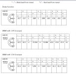
Dont see any specs or dents in the keratherm, believe Q1 isnt shorting to the chassi
That said, Q2 on the bad channel is noticeably warmer than Q2 on the good channel
Resistance from all but 1 pin on Q1 to chassis is in Kohms..
Both circuits (left and right) total Resistance some where near 500K as well
Did not sse your responses...
Dont see any specs or dents in the keratherm, believe Q1 isnt shorting to the chassi
That said, Q2 on the bad channel is noticeably warmer than Q2 on the good channel
Resistance from all but 1 pin on Q1 to chassis is in Kohms..
Both circuits (left and right) total Resistance some where near 500K as well
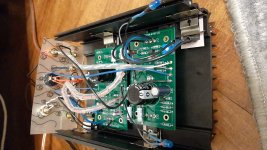
No solder coming through the board around the Q3 holes or the others, stick a bit more on from the side you can see in the photo if its still all bolted down to the heatsink.
Exactly what i was going to say. I was just looking at a 1.6 board I completed and it looks like you've stuffed it with all the correct components save the MOSFETS which I can't clearly see in the pictures. I'd re-flow Q1's solder joints as at least one of them looks suspicious. And as Steve says, redo q3. The smaller transistors are sometimes tricky to get soldered in correctly because I've found folks are afraid to linger too much on those pins.
Your voltages show Q1 with 24 volts on the gate. That can only occur if Q4 was fully conducting and putting the supply voltage on that point.
That condition would give the voltages you are reporting and also cause Q2 to run hot as it is dropping all the supply voltage but still passing around 1 amp current.
So yes, based on the evidence Q4 looks 'bad' but before condemning it be sure to check that the gate is connected correctly (not floating) and that the input coupling cap is correctly polarised.
If you remove Q4 then the midpoint voltage should be at around 18 or 19 volts and both FET's should be cold.
What strikes me as a lead is the source of Q4 is 23.9V and R6 drops it to 22.6V to the gate of Q1 (If im reading it correctly....)
The FET is pulling the voltage down a little because the Gate-Source voltage is a little over the limit for the FET and so the G-S junction may be breaking down (almost certainly non destructively as there isn't enough current to damage it)
Your voltages show Q1 with 24 volts on the gate. That can only occur if Q4 was fully conducting and putting the supply voltage on that point.
That condition would give the voltages you are reporting and also cause Q2 to run hot as it is dropping all the supply voltage but still passing around 1 amp current.
So yes, based on the evidence Q4 looks 'bad' but before condemning it be sure to check that the gate is connected correctly (not floating) and that the input coupling cap is correctly polarised.
If you remove Q4 then the midpoint voltage should be at around 18 or 19 volts and both FET's should be cold.
While you are at it, test Q4 once its removed to ensure its not bad/blown/etc... Before I got this nifty vacuum desoldering station I got into the habit of testing each transistor BEFORE I soldered it in because it could be quite a PITA/mess desoldering. 🙂
--Tom
All, thank you for the responses! Will Absolutely follow the direction given after i get a good night's sleep... eager to resolve this, will at first light... stay tuned
All,
I did re-solder most connections and at least reheated to reflow.
I did add solder to the top of every connection I could as well before my rushed "What strikes me as a lead" response..
What a PITA getting Q4 out!!! I now know I need snippers that DONT crush soft metal... Wound up leaving 1/32"s worth of a leg in the board... Guess I need a mighty fine drill bit now 😡
Anyhow, I tested what was left of the LSK170. As I have never tested a transistor, I hit you tube... Thought I had it, but the 2nd video went over JFET and had me a tad confused.. A few more videos later and I am more unsure of what I thought I understood.
Figured Id measure and keep track of my results... Than I hear about DMM's measuring ohms may not have enough voltage, than I see "Use a Diode Meter"
SO, now I have 3 sets of results that I can make little to no sense of... I thought a PNP JFET will conduct from the drain and source IF the gate has a negative voltage ? If that's correct, than I "think" the part is blown, but I look again at the results and may be think its ok. I cant make heads or tails of this...
Attachments
It's not easy checking FET's if you are not used to doing so. They are such high impedance devices that the floating gate can pick up charge and turn the thing on making it look like it is short circuit.
The JFET is an N channel (we don't call them NPN or PNP) but confusingly for N channel FET's the arrow points inward, and outward for P channel.
If you have an ordinary NPN small signal transistor (like the BC547 etc) then I think that would work as a test to prove the rest of the amp was OK.
Collector would go to the supply and the emitter to R6 and R9. Base to where the gate was. If you try this then just tag it lightly to the board, don't fit it as permanent.
The bias preset would need to be turned nearly to one end but I think it would bias up OK and all work.
To remove a transistor like this don't be afraid to put more solder on and quickly heat all three legs while pulling the device out.
Update.
Ordered a spare kit, will have the parts in a few days (I hope)...
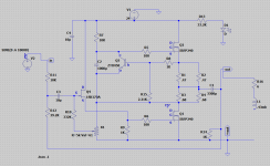
Wifey left for her sisters 🙂 Had a day of learning LTSpice...
Drew up the 1.6 board, Ill be dipped in flux, it works lol..
Now to break things until I find out exactly what went wrong with my channel...
Since this is literally day 1 using LTSpice (Or any circuit design software), I think I made good progress.. I had to create a pot, and added the txt ext so I could upload here...
Ordered a spare kit, will have the parts in a few days (I hope)...
Wifey left for her sisters 🙂 Had a day of learning LTSpice...
Drew up the 1.6 board, Ill be dipped in flux, it works lol..
Now to break things until I find out exactly what went wrong with my channel...
Since this is literally day 1 using LTSpice (Or any circuit design software), I think I made good progress.. I had to create a pot, and added the txt ext so I could upload here...
Attachments
Last edited:
 It took me about twelve months to get that far
 If all i had was the help file, would have taken years! I have always been pretty good at mimicking what someone is doing, YouTube and pause. Add that to the fact that there was no circuit design, all i have done is proven that im further up the rung than say a monkey lolol... but ty for the kind words...
So, i guess I need to know how parts behave and there properties when they break down... surprised there isn't a library of these... take a jfet or mosfet for instance, i would imagine they just dont open the circuit, but conduct more or less than they should and in wrong directions.. while I have the most basic understanding Pf how they behave when functioning, the lack of experience with them comes with a huge disadvantage...
So, i guess I need to know how parts behave and there properties when they break down... surprised there isn't a library of these... take a jfet or mosfet for instance, i would imagine they just dont open the circuit, but conduct more or less than they should and in wrong directions.. while I have the most basic understanding Pf how they behave when functioning, the lack of experience with them comes with a huge disadvantage...
Semiconductors tend to fail in fairly predictable ways tbh but translating that into LTspice is not easy. A lot comes from experience I'm afraid and seeing how certain devices perform in the real world.
Things LTspice fails spectacularly on things like a transistor fitted incorrectly. A real Base/Emitter junction for example would behave more like a 6 to 9 volt Zener diode if reverse biased, LT just behaves like a perfect diode in that scenario.
So you need to think outside the box when looking at how failed parts or incorrectly fitted parts might effect a circuit in simulation.
You can certainly use the simulation to see how an incorrect value or an open connection on a part might effect something.
Hello to all. ACA V1.8 was my first diy build and want to share some incidents I had.. I ordered the kit and the power supply from the store but not the chassis. I had some issues at Turkish customs, as expected, so it was the right choice not to order the chassis (invoice from US, payment to US, chassis shipped from Italy, will be a mess in customs 🙂 ) Also given the fact that I had flied to Bologna IT couple of times per month before Covid, and Hifi 2000 is in Bologna, I postponed the beautiful Hifi chassis for a while..
I found a Bose auto amp chassis from my friend for the task.. Stuffing/soldering the pcb went pretty well by the help of the build guide (thanks for that again). It would be great if the chassis were 1 inch wider because I realised that I had to reposition one of the mosfets 🙁 So I decided to install one of them under the board and that gave me a big headache at the end.. I bolted one of the mosfets into the bottom of the chassis, then put the pcb onto it and soldered pins from the top..but with my "clever" ! positioning pins 1 & 3 were inverted! I realised this during dc balance since there was no voltage change when I turned the pot 🙁 I desoldered the mosfets and installed them to a remote location and connected them to the pcb with wires.. and walla, the amp worked dispite my torture on mosfets! I was worried they were fried with the wrong connection..
Asil
Attachments
Replaced Q4 and now have 12v!
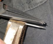
I temporarily soldered the legs to the board as if it was a surface mount component, to troubleshoot.. do i leave it standing tall or shoild I try and drill out the miniscule piece that broke off?
I temporarily soldered the legs to the board as if it was a surface mount component, to troubleshoot.. do i leave it standing tall or shoild I try and drill out the miniscule piece that broke off?
Glad it is sorted. A faulty component is very unusual...
Do not drill it out. Try using a cocktail stick to push the 'bit' out. Make it thin enough to just fit and go right through the hole, apply a little extra solder and pop it through the board. Let it cool and then remove the stick. You can clear the other holes too if necessary.
Do not drill it out. Try using a cocktail stick to push the 'bit' out. Make it thin enough to just fit and go right through the hole, apply a little extra solder and pop it through the board. Let it cool and then remove the stick. You can clear the other holes too if necessary.
Glad it is sorted. A faulty component is very unusual...
Do not drill it out. Try using a cocktail stick to push the 'bit' out. Make it thin enough to just fit and go right through the hole, apply a little extra solder and pop it through the board. Let it cool and then remove the stick. You can clear the other holes too if necessary.
I bought one of those inexpensive component testers, the old ls170 tested as two diodes.. while the new part came up as a transistor...
I will give the cocktail stick a try but worry as the old snippers i used crushed as they cut, (Note to any new at this, Get good sharp snips before you start soldering!) I "thought" i could get it out until the leg broke.. i did have heat on the back side and was pulling from the front when it happened.. will add a little puddle to the back and try to push from the front..
Cant wait to hear it!
Glad it is sorted. A faulty component is very unusual...
Do not drill it out. Try using a cocktail stick to push the 'bit' out. Make it thin enough to just fit and go right through the hole, apply a little extra solder and pop it through the board. Let it cool and then remove the stick. You can clear the other holes too if necessary.
This is why I broke down and got a solder removal station. I used the manual solder sucker forever, and this thing was a godsend when I got mine. You vacuum out ALL the solder. Once you do this, you can see the pin and can wiggle it out - and you might have to snip off the bit above the board. Push it in/out of the hole or rock it back and forth but be careful to not damage the board or the traces/plane. At worst, snip the pins off the transistor from below if you need to - the part is toast. Do these things and be patient because you don't want to damage the board or the layer inside, the holes, etc... and this is why it was righty pointed out above to not drill out the holes. You ruin the conductor that lines the hole, and potentially drill across into the ground plane etc... Just don't do it. 🙂
the old ls170 tested as two diodes.. while the new part came up as a transistor...!
Just for curiosity... the voltage measured on R10 that biases the gate of the FET should measure the same on both ends... however in practice a DVM will pull the voltage at the gate down a tiny little bit.
If you have doubts on the replacement then see if the voltage at the gate is similar to the other end. If the end that goes to the preset is a lot higher... 😱 then you may well have an NPN transistor and not a FET.
Very good news 😀
Managed to get the stuck pin out... Took a brad, cut the head off, chucked it in my drill and filed it down... 1 Vise grip later, and heating it was able to easily push the broken leg out enough to get a grip with pliers, some more heat and boom...
Going to save that make shift tool 😎
Turned on the amp, waited 10 min to get to temperature and both channels balanced to as close as I can get to 12V
Too tired to set up the amp tonight, up since 4AM... Hopefully tomorrow
I will get to hear what it can do... Stay Tuned
Attachments
- Home
- The diyAudio Store
- Amp Camp Amp Kit 1.6/1.8