I built a pair of v1.6's and tested each one in stereo while waiting for a set of XLR cables from Blue Jeans Cable. They sounded good in stereo on my MJK OB's with H-frames. As expected, I had turn up the volume on the OPPO BD-105 to get the sound, it was amazing.
As monoblocks they really sing. Thank you to NP and all the others that continue to make this happening happen. Bill
As monoblocks they really sing. Thank you to NP and all the others that continue to make this happening happen. Bill
I unscrewed the board that wasn't working, flipped it over and just re-melted every single solder joint - she works now!
okay last question: when it's playing, it sounds great, however when nothing is playing I can hear a very slight hiss from the speakers, is that normal for these amps?
okay last question: when it's playing, it sounds great, however when nothing is playing I can hear a very slight hiss from the speakers, is that normal for these amps?
Agreed. Saw that today as well.Actually PcChip is correct, there is a slight bow to the silver brackets from front to back.
I would have tried roughing the pieces together at that point but realized I was short one silver screw, so will head to the local hardware store this week. No worries. I installed all rear panel parts instead and set up the ground buss wire.
Confused?
I Jason, My questions is about the top of the DPDT Switch, from the V1.8 wiring guide are the two top terminals supposed to be tied together? Or are they not connected to anything?
Thanks for your Future support
Mark
For the rear switch, almost any on-off-on DPDT switch will do.
For those building the V1.8 using V1.6 instructions, attached is a direct comparison that clearly shows the differences.
As the differences are very slight, I will rename this thread "V1.6 / V1.8".
I Jason, My questions is about the top of the DPDT Switch, from the V1.8 wiring guide are the two top terminals supposed to be tied together? Or are they not connected to anything?
Thanks for your Future support
Mark
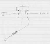
Yes they are supposed to be 'tied'. This is for parallel mode.
When the switch toggle is down the White and Red inputs are joined together via the link.
See the diagram.
Likewise when the switch toggle is in the central position there are no connection. Stereo mode.
When the switch toggle is in the up position, the right half of the switch connects the 39K resistor (from the speaker terminal) to the Red input socket. Bridge mode.
Hope that helps?
Attachments
On to the Build 🙂.
Hi Alan4411,
Thank you for clarifying that for me.
I'll start by upgrading my original 1.6. Then its on to the 1.8 build.
You and everyone here have been a great inspiration.
Mark
Hi Alan4411,
Thank you for clarifying that for me.
I'll start by upgrading my original 1.6. Then its on to the 1.8 build.
You and everyone here have been a great inspiration.
Mark
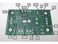
ACA 1.8 PCB stuffing aid
I have not put together a kit for a while, so I took one of the 1.6 build guide photos and edited it to show the resistor values for the 1.8 build. (Only one change.) This saves a mental step or two when checking resistances before soldering. I'm doing 4 boards so I'm looking for _any_ help to avoid resoldering.
The very small resistors are the problem (so far). I'll edit this further if necessary for me, or if encouraged.
annotated ACA pcb from site.jpeg - Google Drive
I was toolin along on the 1.6 build guide and realized I should pay careful attention to the new 1.8 wiring diagram.
So just to confirm what I see in the diagram:
For reference, 1.8 wiring https://cdn.shopify.com/s/files/1/1006/5046/files/ACA_wiring_-_All_Together_-_V18.pdf?v=1593415056
As far as the 3-way switch:
top position: pins tied together
mid position: use left and right input
bottom pos: a single pin to a 39K resistor to a - output from one channel board.
Am I reading this correctly?
Thanks!
Am I reading this correctly?Thanks!
Oh for want of an edit button - momentary lapse of reason
 - yes I'm reading it correctly.
 Carry on.
balancing dc voltage snafu....
Hello all!
Woke up early today and solderd the last few wires for the 1.8 kit...
Running out of time (had to get to work) i plugged in the power to set the voltage at Q1 and one side was able to get close enough to the suggested 12v. With only a minute or two left saw that Q1 on the other side was only giving me milli volts ..
When i get back home today or tomorrow will run through the trouble shooting image and check my values, that said does anyone here know of what else to look for?
Thanks!
Glenn
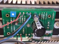
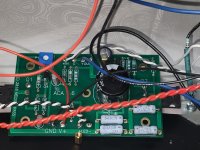
Can anyone share an image of the backside of the 1.8 board?
Tracking back my problem I have only 5.8 volts to R7. I have nearly 24 at Q2 drain and Q4 drain... somethings not quite right on my left channel..
Tracking back my problem I have only 5.8 volts to R7. I have nearly 24 at Q2 drain and Q4 drain... somethings not quite right on my left channel..
Here is a picture of the rear of the board. Not sure it helps.
Better if you post pictures of your faulty board?
24 volts on the Drain of Q1 and Q4 is correct.
With 5.8 volts on R7 check,
Q3 is the correct part (not Q4 by mistake) and inserted the right way round.
C2 is the correct way round.
R7 is the 10k ohm resistor. That it is soldered in with no 'cold' joints.
Attachments
Last edited:
Bummer !
Q3 is correct (So is Q4 lol)
C2 has the p towards the positive
R7 measured damn near 10K ohms...
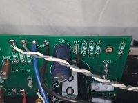
Attached is the problem child...
How can I check a transistor while in a circuit ?
Have near zero ohms from the legs of Q3 to any other points,
so its soldered well enough...
Time for bed.. the Am comes way too fast these days... and thanks again for your help...
EDIT--
I uploaded the wrong pic... The first is my right channel, working
the next two are my left channel and the problem one
Q3 is correct (So is Q4 lol)
C2 has the p towards the positive
R7 measured damn near 10K ohms...
Attached is the problem child...
How can I check a transistor while in a circuit ?
Have near zero ohms from the legs of Q3 to any other points,
so its soldered well enough...
Time for bed.. the Am comes way too fast these days... and thanks again for your help...
EDIT--
I uploaded the wrong pic... The first is my right channel, working
the next two are my left channel and the problem one
Attachments
Last edited:
No solder coming through the board around the Q3 holes or the others, stick a bit more on from the side you can see in the photo if its still all bolted down to the heatsink.
Ok, will try.... but..
I tested the resistance from every pin i could to the next connection in the board and have pretty much zero ohms, there was one connection that gave me .6 or so ohms, i buttered that up and am reasonably sure its not the issue (i really ish it was)..
Willing to try anything, hopefully can wake up a few hours early tomorrow...
Every thing looks in the right place.
Your soldering is a little 'shallow'. Ideally the solder should show on the front (component) side of the board as well. Best to resolder all the joints now it is off the heat sink.
Going back to your initial post #771, did you notice if both Q1 and Q2 were both getting hot?
I wonder if Q1 D was shorted to the chassis. Maybe a blob of solder got stuck in the kerotherm pad? Have a careful look. The Drain is also the metal tab.
So resolder the board, remount the assembly back on the chassis. Check the Drain of Q1 and Q2 are not shorted to the chassis / GND connection. Try again.
Do Not be tempted to switch on with the assembly off the chassis.
The only thing I can think of that could cause this... no voltage at the midrail and 5.8 volts on R7 (I assume the other end does have +24 present) would be Q3.
Make sure the device is marked as per the one in the good channel.
Check it in circuit initially and using the diode range range on your meter. Be careful to observe polarity of the meter leads when measuring and compare it to Q3 in the good channel.
Does it read similar or does it read either 'low' in any directions or more unusually, does it read 'opposite' in results to the good channel with regard to lead polarity.
Trying to see if I can order 1 channel, pcb and all components...
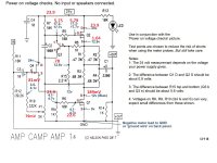
Attached is my last ditch effort and probably great fodder for anyone who loves troubleshooting this stuff.. I have a very basic knowledge of electronics, and this is well over my head....
The values in red are all in volts unless specified.
What strikes me as a lead is the source of Q4 is 23.9V and R6 drops it to 22.6V to the gate of Q1 (If im reading it correctly....)
I didnt see a bridge across the D&S of Q4, could it be bad ?
Attachments
- Home
- The diyAudio Store
- Amp Camp Amp Kit 1.6/1.8