Oh no, I was afraid that would be the answer! Based on the readings I have made would anyone have a best guess on which order to take them out and test?then pull them out and test
road to hell is tiled with best guesses
damn thing is having 4 semiconductors ....... it can't be hard to find which one is not conductor any more
🙂
damn thing is having 4 semiconductors ....... it can't be hard to find which one is not conductor any more
🙂
My soldering is bad, my desoldering much worse, just thought there might be an obvious place to start but thanks anywayit can't be hard to find which one is not conductor any more
I would say that careful voltage checks should reveal the problem here. Always aim to disturb everything as little possible while gathering evidence.
If you measure and record the voltages at key points it should provide a clue.
You could begin by carefully measuring on all 6 of the output transistor leads.
If you post the results here we can take a look 🙂
If you measure and record the voltages at key points it should provide a clue.
You could begin by carefully measuring on all 6 of the output transistor leads.
If you post the results here we can take a look 🙂
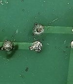
It seems to me that the PCB is a little burnt close to Q2 and it doesn't seem like it is because of a soldering iron being too close.
I saw that burn mark also. Thought it might just be a shadow, but it does seem to be blackened on the PCB.
So the cold channel gives the following power on voltages;You could begin by carefully measuring on all 6 of the output transistor leads.
Q1 S=0v, D=7.5V, G=2.78V
Q2 G=7.61v, D=24V, S=7.5V
Hadn't noticed this before and I have just put the board back on the heatsink to take the above voltages but will check later, good spot.It seems to me that the PCB is a little burnt close to Q2 and it doesn't seem like it is because of a soldering iron being too close.
Report Post
Last edited:
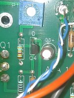
I read yesterday that someone spotted this connection on C3.
Did you re-solder and see if your amp came back to life after? I didn't see any response so maybe you missed that suggestion? You sure are not going to get any current to flow through that junction for very long!
Did you re-solder and see if your amp came back to life after? I didn't see any response so maybe you missed that suggestion? You sure are not going to get any current to flow through that junction for very long!
Attachments
I read yesterday that someone spotted this connection on C3.
Did you re-solder and see if your amp came back to life after? I didn't see any response so maybe you missed that suggestion? You sure are not going to get any current to flow through that junction for very long!
I did miss it, thanks, It looks awful on the photo but didn't spot it when I checked the actual board at the weekend, will resolder tomorrow.
Toshiba K370. I built 2 identical ACAs at the same time, all ran well for several months, the other is still ok.Out of interest (and it might be significant?) what device did you use for the LSK170 / 2SK170 Q4?
Normally they both have a flat front and rounded rear body. The picture shows a clear flat on the rear face.
I read yesterday that someone spotted this connection on C3.
Did you re-solder and see if your amp came back to life after? I didn't see any response so maybe you missed that suggestion? You sure are not going to get any current to flow through that junction for very long!
Alas what I hoped was the simple solution hasn't worked, I reflowed the dodgy joint but still no joy.
That's sad captain, but the brown/burnt area around Q2 is very suspicious, there must have been high currents/temps. I think you can't avoid to desolder the semis and check them. There is also a possibility to check them while in the circuit (amp must be turned off), there are many descriptions in the net, f.e.: #132: How to test MOSFETs with a DMM - a few methods... - YouTube Hope it helps.
So the cold channel gives the following power on voltages;
Q1 S=0v, D=7.5V, G=2.78V
Q2 G=7.61v, D=24V, S=7.5V
Only just got around to this...
First thought is a short or extreme low resistance across C2 which is the 1000uF cap. The transistor Q3 could be at fault as that is across the cap.
A short between base and collector of Q3 would also do this.
First thought is a short or extreme low resistance across C2 which is the 1000uF cap. The transistor Q3 could be at fault as that is across the cap.
A short between base and collector of Q3 would also do this.
That's sad captain, but the brown/burnt area around Q2 is very suspicious, there must have been high currents/temps. I think you can't avoid to desolder the semis and check them. There is also a possibility to check them while in the circuit (amp must be turned off), there are many descriptions in the net, f.e.: #132: How to test MOSFETs with a DMM - a few methods... - YouTube Hope it helps.
__________________
Thanks chaps, I will check for shorts first then the mosfets.
how hard will it be to simply replace all active devices and start over?
__________________
It was my original plan and in the end it may well be what I end up doing but why not learn something along the way? I know also that people will be reading this thread in years to come so my little problem may help others.
could be a bad soldering point - lost or bad contact after a few weeks........
i would carefully solder again all bad looking points .
i would carefully solder again all bad looking points .
- Home
- Amplifiers
- Pass Labs
- Amp Camp Amp - ACA