Hugh@:
Hi, thank you very much for your explanation. Although the truth has surprised me, I did not expect such a low value.
Regards
Hi, thank you very much for your explanation. Although the truth has surprised me, I did not expect such a low value.
Regards

Hi Danny,
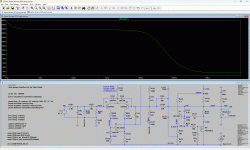
I checked with LTSpice and YES, you are 100% correct the Zin of the AN39/20 is 21.4k. This is far higher than I'd expected
based on the configuration of a long tailed pair on the net, so it seems to me it was not correct.
An interesting lesson to learn!
Thank you for drawing my attention to it. Appreciated..... and Happy New Year!
Cheers,
Hugh
I checked with LTSpice and YES, you are 100% correct the Zin of the AN39/20 is 21.4k. This is far higher than I'd expected
based on the configuration of a long tailed pair on the net, so it seems to me it was not correct.
An interesting lesson to learn!
Great to hear, Hugh. 👍 That means an AN can probably take a tube preamp (for those who are that way inclined 🙂 ).
Hi Hugh,
Thanks for showing us how to calculate the input impedance resulting from the base current. I suspected as such but didn’t know how to quickly calculate it. 3k4 is kinda low for input impedance, but most preamps or opamps can drive that no problem. Does that affect the value of the input coupling cap though in order to get a low pass filter deep enough?
Happy new year! It’s still only about 9pm here on the East Coast.
Edit: just saw your later post - so a LTSpice sim confirms that it is 21.4K? We are alright then.
Perfect! Thank you for shedding light on this important piece of information.
Good year and good luck to all of you!!!
Good year and good luck to all of you!!!
Thanks to LTspice for calculating the influence of all the components in a flick of a switch 🙂I checked with LTSpice and YES, you are 100% correct the Zin of the AN39/20 is 21.4k.
Happy New Year!
Hello everybody.
Have a happy and healthy new year.
Yesterday, during a rough time of soldering the snubber boards' smd parts, I was tempted to create something more simple for my next AN build.
A pcb with no smds, no molex connectors, no special tools for soldering and crimping and diode easy orientation for N and P mosfets.
Note that the mosfet is on the other side of the pcb, on its ceramic or silicone insulation board.
The dimentions of the board are 50mm X 19mm.
And here it is.
Something like this Metanastis? This is my original pcb for the Alpha many years ago...... all thru hole, as you can see. This was the original amp based on the output stage of the Aleph J which I changed for the AN (and I thought was superior to the Aleph idea).
I particularly enjoy layout, and love the graphic aspect. But I don't like the building much, and never did build it. I first heard the AN in AndyR's home a couple of years later. At this point I was moving ahead with more development of the Maya, which is now in Version IV, and rated to 200W.
Thank you for building the AN. It is a lovely amplifier and I have a real soft spot for it.......
Happy New Year to you and all Greek audiophiles!
Hugh Dean
You don’t have to use the Molex connector on the snubber boards. If you notice from Post 1 of this thread, I soldered wires directly to the pads (on top side):Hello everybody.
Have a happy and healthy new year.
Yesterday, during a rough time of soldering the snubber boards' smd parts, I was tempted to create something more simple for my next AN build.
A pcb with no smds, no molex connectors, no special tools for soldering and crimping and diode easy orientation for N and P mosfets.
Note that the mosfet is on the other side of the pcb, on its ceramic or silicone insulation board.
The dimentions of the board are 50mm X 19mm.
And here it is.View attachment 1255285
You do have mini-MELF parts but they are easy to solder. Just hold still with tweezers while you reflow a blob of preinstalled solder on one pad.
@xrk971
Yesterday night I soldered the smds using my weller soldering station and a very thin and sharp tip. It took me a long time to solder and align the 4 snubber parts because I haven't got the special hot air gun and special solder for smds and I was pissed off🤣. Your snubber boards are professionally designed. A piece of art for many DIYers. I am one of them but I dislike smd parts. Molex too.
Have a happy and healthy new year.
You can do big SMD MELF with an iron and small chisel tip and plain solder.
Use solder and iron to pre-tin SMT pad with small blob of solder. Use tweezer to hold part in place on pad. Place chisel tip at corner of part and pad. Solder from pretin pad will melt and wet.
You need good tweezers to do SMT.
Use solder and iron to pre-tin SMT pad with small blob of solder. Use tweezer to hold part in place on pad. Place chisel tip at corner of part and pad. Solder from pretin pad will melt and wet.
You need good tweezers to do SMT.
Yes XRK, it was something like this. A kind of......surgery especially for the alignment😆😆!!! For 30 years in the aerospace industry, I have soldered and disordered thousands of parts. For SMD parts, there were special electronic machines PC controlled for soldering purposes. For disoldering there were soldering absorbing stations. I am sure that in my next smd soldering trial I will be better and better time after time. Thanks for your advice anyway.
Three questions for the 4R build, please.
1. I have soldered four 15V zeners on the snubber boards. Is it OK or they must be 12V ??
2. The gate 100R resistors must be shorted if there will be a snubber board?
3. Do the molex output cables from the main board need to be carried twisted to the snubber board
Thanks a lot.
1. I have soldered four 15V zeners on the snubber boards. Is it OK or they must be 12V ??
2. The gate 100R resistors must be shorted if there will be a snubber board?
3. Do the molex output cables from the main board need to be carried twisted to the snubber board
Thanks a lot.
Last edited:
Hi Meta,
#1 No, the limit of the Vgs is 20V on the datasheets, so 15V is fine.
#2 No, you need to use a gate resistor AND a snubber board (XRK should comfirm this).
#3 I suspect twisting the cables to the snubber board/mosfet board is more resistant to EMI, so YES.
HD
#1 No, the limit of the Vgs is 20V on the datasheets, so 15V is fine.
#2 No, you need to use a gate resistor AND a snubber board (XRK should comfirm this).
#3 I suspect twisting the cables to the snubber board/mosfet board is more resistant to EMI, so YES.
HD
If you use the snubber board then populate the SMT snubber resistor in the helper board and wire a jumper on the main PCB. You don’t need both, but it’s better to have it as close to the pin as possible, hence the small SMT one on the snubber board itself.
3. Do the molex output cables from the main board need to be carried twisted to the snubber board
Thanks a lot.
#3 I suspect twisting the cables to the snubber board/mosfet board is more resistant to EMI, so YES.
Further to Hugh's recommendation - as you have 3 wires ... I suggest braiding them does a better job of EMI protection than just twisting them.
And btw - I used both the 100R Gate res on the main PCB and the 100R SMT res on the Snubber board.
- Home
- Amplifiers
- Solid State
- Alpha Nirvana 39w 8ohm Class A Amp