If you have an op-amp that can do it, why not use it as VAS too?
Because it's not easy to make op-amp to swing from rail to rail. If the whole amp is powered by 15V rails, that's ok.
But if we have OS rails 20V, or 30V, the op-amp can't do it. You can use high voltage op-amp (question asked in post #2178)
or tricks like op-amp with floating ground referenced to the output of the amp,
but these design usually are more difficult to make them stable.
See Elvee's Easy Dump amp for such example.
Maybe this should have it's own thread?
Well, yeah, but I put it here, hoping for Hugh's input and his expertise in shaping the "profile"..
If sims go well, and I do my own build, will start another thread. Or if X kicks me out 🙂
After building three ANs, I need something different....
For now, I'll try to make sure the design is stable (phase margin, etc..), and handles square waves well.
I'm also thinking of replacing R13 with extra 1-transistor buffer, to keep op-amp DC offset at 0V. As it is, value of R13 depends on the rails voltage, and needs to be adjusted if someone wants to change rails voltage.
Last edited:
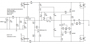
Here a slightly updated version that handles square waves much better,
and ALSO has some FFT shaping RC network added (optional), so the profile is the similar levels like original AN.
Perhaps this effort went little bit too far 🙂
Feel free to play with values of R6/C13 to adjust the harmonics levels.
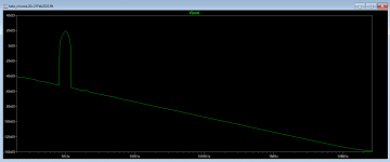
This fft plot with current value sof R6/C13 is included only as an educational exercise, I wouldn't keep it "as is".
Even with this straight-line profile, Thd level stays at 0.005% level at full power, which is very interesting behavior.
It didn't get much worse, as I expected.
Slew rate also seems to be slightly (20%) improved over original AN.
and ALSO has some FFT shaping RC network added (optional), so the profile is the similar levels like original AN.
Perhaps this effort went little bit too far 🙂
Feel free to play with values of R6/C13 to adjust the harmonics levels.
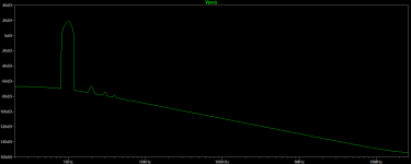
This fft plot with current value sof R6/C13 is included only as an educational exercise, I wouldn't keep it "as is".
Even with this straight-line profile, Thd level stays at 0.005% level at full power, which is very interesting behavior.
It didn't get much worse, as I expected.
Slew rate also seems to be slightly (20%) improved over original AN.
Attachments
Last edited:
Yes you are correct - the cascode above the JFET is a local feedback. I meant zero feedback from output stage back to input stage.What you mean by "zero feedback"? Just by adding bootstrap, you are creating strong feedback loop.
Even emitter (or source) resistors create feedback loops too.
Regardless of that, the Lufo profile looks as good as it gets....
And here is new and improved version with a buffer (Q1 after the op-amp) mentioned in previous post.
Thd is down, R6/C13 adjusted for a more reasonable FFT profile.
Gain can be set by R4 (higher value = less gain). Rails can be increased to, say 27V, without changing anything.
C5 is most likely not needed - prototype build will tell us if output DC offset is close to 0V. If not, C5 will be needed.
Thd is down, R6/C13 adjusted for a more reasonable FFT profile.
Gain can be set by R4 (higher value = less gain). Rails can be increased to, say 27V, without changing anything.
C5 is most likely not needed - prototype build will tell us if output DC offset is close to 0V. If not, C5 will be needed.
Attachments
Last edited:

Hi, any chance of single side pcb for home etching maybe? I think it would attract a lot more interest for building this nice amp.
Hmmm, perhaps we could ask Prasi? He is the undisputed single layer designer here...... Prasi? Please, a slight change on the original Alpha Nirvana with this IC front end? What do you think?
Hugh
Hugh
Wow. Pretty amazing developments. I am watching with curiosity from afar since I have an AN in my stable playing and working great.
I would include the option of the end user substituting their own power supply (+/- 15V DC) for the JFET IC front end, i.e. the option of using D1, D2, C3, C4, R5, R14 or not.
Any options for a differential front end or differential to SE conversion using a JFET IC? Just asking.
Of course at +/-27V supplies, I would try higher source resistors (i.e. 0.22 ohms like in original AN) to keep dissipation at sane levels (and 8/6 ohm loads). With this new schematic at +/- 20V rails and 0.15 ohm source resistors, it seems better for 4 ohm loads.
Thanks Minek123 and Hugh/AKSA for all your hard work!
@prasi ... how you doin buddy?!
Best,
Anand.
I would try higher source resistors (i.e. 0.22 ohms like in original AN) to keep dissipation at sane levels (and 8/6 ohm loads).
With this new schematic at +/- 20V rails and 0.15 ohm source resistors, it seems better for 4 ohm loads.
Right!
Q4 limits the idle current of the OS. Source resistors: higher values = less idle current.
With 20V rails and 0.15 Ohm resistors idle current will be limited to 2.36 A (50W dissipation per FET at idle).
With 20V rails and 0.22 Ohm resistors idle current will be limited to 1.6 A (35W dissipation per FET at idle).
My choice for 8 Ohm speaker would be 0.22 Ohm, 1.6A seems plenty enough.
I think for 4 Ohm speaker, 0.22 Ohm resistors still should be OK, but gain needs to be lowered (E.g. R4 = 2k2)
Unless Hugh have some other reasons to use different values for these resistors (beside controlling idle current) ?
Generally speaking, source resistors are adding Thd, and the lower value, the better.
Usually, for a single pair of HexFets they can be skipped completely, but here we need them as 'current sensors'.
Perhaps they could have been located in the drains instead, but this would complicate further idle current control/limiter (Q4).
I make your FFT at +20dBU (12.5W//8R) very good and with H2 -90dB and H5 -120dB it couldn't get any better! Good circuit, congratulations!
Looks great! Hugh, can you share what did you do?
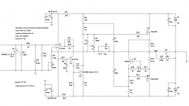
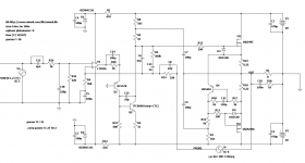
Here is latest schematic:
1) Q1 cascode simplified (base of Q1 can be connected directly to the ground, one resistor and LED eliminated)
Q1 could be pretty much any small PNP BJT
2) 12V Zener protection for FET gates added.
3) source resistors changed to 0.22 Ohm
One more thing left to test - clipping behavior, and capacitance loads.
I'll be designing my own PCB (and I'll publish it), but most likely it will be double sided.
I'm planing to re-use existing pre-drilled chassis from another amp, so the shape of my PCB (it's going to be small)
might not be optimal for other builders...
Attachments
One thing you could do if you design a new PCB is to make an option to connect C7 to M1 drain? I think that was an improvement on my AN, so maybe you want to try it? (lower output impedance)
Did you try the same trick with C9 ?One thing you could do if you design a new PCB is to make an option to connect C7 to M1 drain? I think that was an improvement on my AN, so maybe you want to try it? (lower output impedance)
Super cool twist to the Alpha Nirvana Minek and Hugh!
If a pcb is developed and shared, can the mounting holes and Molex headers for mosfet flying leads be pin compatable and located in the same position as original AN boards so existing AN builders can “plug and play” this new version?
If a pcb is developed and shared, can the mounting holes and Molex headers for mosfet flying leads be pin compatable and located in the same position as original AN boards so existing AN builders can “plug and play” this new version?
Practical advantages of replacing LTP input stage with Jfet op-amp is that we are getting matched and thermally coupled Jfet LTP practically for free.
Any op-amp's input LTP (even in the cheapest op-amps) will be of better quality than discrete LTP.
TL071 op-amp was $1 (at Digikey) last time I ordered it, and there is nothing to adjust/measure (no trimmers).
DC output offset should be very close to zero without any extra effort.
Using op-amp allows for high gain loop, and more NFB, which leads to minimal distortions.
In which case, JPS64 would be the one for the Beta Nirvana layout. He’s quite busy lately though…Super cool twist to the Alpha Nirvana Minek and Hugh!
If a pcb is developed and shared, can the mounting holes and Molex headers for mosfet flying leads be pin compatable and located in the same position as original AN boards so existing AN builders can “plug and play” this new version?
Prasi is our only hope 🙂
The ideal for most of builders would be backward-compatible, single layer board.
Doesn't have to be based on the JPS64's board, as long as it has the holes for all connectors in the same places.
The ideal for most of builders would be backward-compatible, single layer board.
Doesn't have to be based on the JPS64's board, as long as it has the holes for all connectors in the same places.
Hi Folks, to keep things less confusing, there is a new thread for the Beta Nirvana here:
https://www.diyaudio.com/community/threads/beta-nirvana-class-a-amp.383388/
If the moderators can be so kind as to move the previous posts related to this new amp over to the new thread, that would be appreciated.
Thank you Minek for your creative power here.
https://www.diyaudio.com/community/threads/beta-nirvana-class-a-amp.383388/
If the moderators can be so kind as to move the previous posts related to this new amp over to the new thread, that would be appreciated.
Thank you Minek for your creative power here.
No, it did not see any change in simulation, so I left it alone. I have only been playing with the values to reduce turn-on thump/offset.Did you try the same trick with C9 ?
Ci sono file gerber o tracce pcb in pdf. Voglio provare a costruire questo amplificatore per vedere come suona
- Home
- Amplifiers
- Solid State
- Alpha Nirvana 39w 8ohm Class A Amp