X, Hugh,
Need some advice on the input stage/LTP bias current. I am using KSA 992 BJT's. Is 2.6mA the absolute goal or is anything around 2-3 mA just fine (Hugh's schematic shows 1.9mA but with different BJT's)? I can dial in the offset to be close to 0mV at ~ 2.3mA but at 2.6mA it is more like (-)11 mV. No big deal either way I bet since the dc offset is quite low.
Now on to the other channel!
Best,
Anand.
Hi Anand
If I recall, I think the design goal was circa 2mA so you have it just about right.
This raises an interesting question, X - well, in my mind anyway! 😀
We adjust R113 on the 8R schematic to get DC offset at the spkr terminals as near to 0.0v as we can get it. As Anand has stated, the value of this resistor determines the input stage/LTP bias current.
But surely it's the DC offset that is important here - not the actual bias current? (That's just the result of setting R113 to minimise DC offset?)
Andy
Actually, it is the bias current in the LTP that is more important as we want to operate in the range of the BJT where the linearity is best. This is where it is similar to setting the plate current on a tube amp to get the best performance. That is about as much as I know, Hugh will have a much better answer from a technical standpoint. The DC offset, whether 2mV or 10mV is of no consequence as long as it is under ~20mV. Even 50mV is not a huge deal as that is less than 1/3rd mW into 8ohms. Nothing to worry about.
Hi Anand,
Just so happens I am setting the LTP bias current also. I prioritized the 2.6mA number over output DC offset. Using the R113 trimpot I adjusted voltage across R111 to 8.75v.
8.75/3300 = 2.65mA
Both channels adjusted the same way yields less than <10mV offset Right and <4mV offset Left. Definitely nothing to loose sleep over 🙂
Attachments

Actually, it is the bias current in the LTP that is more important as we want to operate in the range of the BJT where the linearity is best. This is where it is similar to setting the plate current on a tube amp to get the best performance. That is about as much as I know, Hugh will have a much better answer from a technical standpoint. The DC offset, whether 2mV or 10mV is of no consequence as long as it is under ~20mV. Even 50mV is not a huge deal as that is less than 1/3rd mW into 8ohms. Nothing to worry about.
Aah, OK - thanks for that info, X.
Andy
Well the actual question comes down to what really should be the input LTP bias current range for best linearity? Is 2.3mA (which gives me 0mV offset) a compromise compared to 2.6mA?
DC offset whether 10, 20 or 50mV is really immaterial. And this is from a fella who has 96 dB sensitive speakers and an SSR on the output of the amp. Just as X has stated.
Best,
Anand.
DC offset whether 10, 20 or 50mV is really immaterial. And this is from a fella who has 96 dB sensitive speakers and an SSR on the output of the amp. Just as X has stated.
Best,
Anand.
Looks like KSA992 hfe start drooping at abt 1mA, but then there are other factors too. Adjusting it while watching distortion FFT could be an interesting exercise 🙂

2N5401 is shows better characteristics in 2mA...3mA range.
Hugh's original schematic was using 2N5401, not KSA992.
On the other hand, I guess running LTP in 1mA range shouldn't hurt anything.... Most of amps stick to 1mA rule.
Perhaps Hugh can give us more details about this...
In my build, I used BC556C, at 1.2mA.
Hugh's original schematic was using 2N5401, not KSA992.
On the other hand, I guess running LTP in 1mA range shouldn't hurt anything.... Most of amps stick to 1mA rule.
Perhaps Hugh can give us more details about this...
In my build, I used BC556C, at 1.2mA.
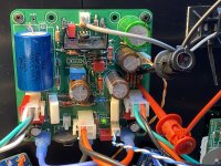
Noob question. X used MELF carbon resistors (100R and 47R) on the snubber boards. Can "normal" chip smd resistors be used here without regrets? I am trying to source BOM parts from 4 different suppliers. One heck of a exercise with component shortages all over.
Why use two gate resistors? There are gate resistors on the main PCB too. I jumped the pads on the snubber boards because of this.
Way earlier in the thread (i.e 1st 10-15 pages) I think X had selected the MELF resistors for ease of soldering but also due to durability in combating parasitics and oscillation potentials when implemented as part of a snubber circuit.Noob question. X used MELF carbon resistors (100R and 47R) on the snubber boards. Can "normal" chip smd resistors be used here without regrets? I am trying to source BOM parts from 4 different suppliers. One heck of a exercise with component shortages all over.
Take care in properly implementing the diode in the snubber. It's mounted one way on the N Channel and the other way on the P channel:
https://www.diyaudio.com/community/...-8ohm-class-a-amp.344540/page-10#post-5986284
Best,
Anand.
There are gate resistors on the main PCB too.
Gate resistors should be as close to the gate, as possible.
If output devices are soldered directly to the PCB, it's OK to have gate resistors on PCB.
But, if output devices are connected by (longer) wires, gate resistor should be "on the transistor", not on the PCB.
Thank you, this was new to me, I have not built many fet amps. Is there a short and simple explanation to this?
Yes, no worries. Regular chip resistors are fine. Just don’t use thick film. Metal thin film is best. In version cases, thick film has more odd order distortion (I found that when used on feedback resistor of Aksa Lender preamp).Noob question. X used MELF carbon resistors (100R and 47R) on the snubber boards. Can "normal" chip smd resistors be used here without regrets? I am trying to source BOM parts from 4 different suppliers. One heck of a exercise with component shortages all over.
You want snubbers mounted as close to the transistor pins as possible to absorb any HF energy that could be oscillating before it reaches the transistor. Longer wire with resistor on other end allows wire to pick up RF.
Sorry, R101 on the snubber board can be jumpered if the gate resistors on the main board are used.
R102/C102 are the snubber components between mosfet G/D legs. These parts should be installed along with V101.
R102/C102 are the snubber components between mosfet G/D legs. These parts should be installed along with V101.
Thank you all for clarifying.
Yes, thank you Anand - very important and I made a big note of this. X’s build photos are a great help too.Take care in properly implementing the diode in the snubber. It's mounted one way on the N Channel and the other way on the P channel:
https://www.diyaudio.com/community/...-8ohm-class-a-amp.344540/page-10#post-5986284
Best,
Anand.
Vunce, your answer had me worried and look at the schematic again. Yes, vice versa - if using the gate resistors (R101) on the snubber boards (preferred option), then R133, R135 on the main boards must be jumpered. I almost missed this. See post #1810Sorry, R101 on the snubber board can be jumpered if the gate resistors on the main board are used.
R102/C102 are the snubber components between mosfet G/D legs. These parts should be installed along with V101.
twocents,
See post 1816 for additional clarification. I would say if you are jumpering R133, R135 on the main pcb then the gate resistor R101 is a necessity and yes the preferred method. Gate stoppers (similar to grid stoppers in tubes) are best applied very near the gate itself. That being said if you already have 100R on R133/R135 and another 100R on R101 the amp won't misbehave and it is doubtful it will make a sonic difference. But for purists...
On my first board, I ran a FRA/Bode plot analysis, and it is flat from 10Hz to ~ 200khz (-3dB) with a 10uf input capacitor. Phase was flat and -7 degrees at 20khz, pretty close to simulation (1st post of this thread).
R102,C102, and V101 (properly oriented) on the snubber pcb must be used since this amp intrinsically uses MOSFETS on fly leads. There is a convenience to this, although, I will admit this is the only amplifier in the XRK arsenal that uses this feature. In order to make it more dejure, we need more designs applying this 😉. Or else, it appears as a novelty at best.
I will await Hugh's comment on the input LTP bias current recommendation for KSA992's.
Best,
Anand.
Last edited:
Anand
I originally chose 2N5401 and 2ma. Then X preferred A992 because they had higher beta with very similar current. Noise is not an issue with this amp; it is very quiet with stage current of 4.25ma.
HD
I originally chose 2N5401 and 2ma. Then X preferred A992 because they had higher beta with very similar current. Noise is not an issue with this amp; it is very quiet with stage current of 4.25ma.
HD
- Home
- Amplifiers
- Solid State
- Alpha Nirvana 39w 8ohm Class A Amp