Series "termination" should be placed at the source end if it's a point to point connection. It's not end-of-the-world critical, though. I don't care what some crazy person at AKM thinks is correct, putting it in the middle makes no sense. All I2S lines should have the series resistance.
I agree with you. For it to be most effective and minimize ringing on the line. I remember when we were using Xilinx parts, it was an option in the I/O cell, it saved a lot of resistors on the board.Series "termination" should be placed at the source end if it's a point to point connection.
Does AKM supply IBIS models for their I/O's? I guess you would have to contact them, maybe sign an NDA, who knows, I have never worked with that outfit.
Rick -- Haven't seen anything on IBIS models for the AKM chips, either way it looks like eispice is the only open source tool that can handle these models. Maybe there's a way to convert HDL models to IBIS models that might work for this application. Unfortunately, can't find any information on the output impedance from the DIR chip in the datasheet, am I just searching for the wrong thing or can we assume Z = 50?
It’s not that critical. It’s not going to be 50 ohms unless it has an internal resistor, I’d just put something like 33 ohms on the board and go with it.
I would add.. Also the line impedance is not something cast in stone.. Higher line impedance eases up on termination load. Until you stay on the board, do not go out to external interconnects. A limit is that on multilayer boards starts to be a thin trace..
I would add.. Also the line impedance is not something cast in stone.. Higher line impedance eases up on termination load. Until you stay on the board, do not go out to external interconnects. A limit is that on multilayer boards starts to be a thin trace..
Yes, if the signal is critical enough to need to be treated as a transmission line, it probably shouldn't be a single-ended LVCMOS signal if the trace is anything but very short. I would prefer to use differential LVPECL, HCSL, or LVDS with a controlled impedance PCB and actual termination.
Joseph, not sure I understand what you mean. Chris, TI seems to use SMA connectors and transmission lines for LVCMOS signals, as mentioned here: http://www.ti.com/lit/ug/snou125/snou125.pdf . I plan on using controlled impedance PCBs for this project regardless, many fab houses seem to offer them these days at no extra cost. Are you recommending that I use something equivalent to the TP teleporter to convert I2S LVCMOS to LVDS and back again? Worried about the jitter that this could possibly add to the system, but would give the advantage of being able to run the differential signals over the PCIe bus, as described in the spec.
Used LVDS on my 2nd dac project for compatibility with LMK01000. Worked okay in terms of jitter likely because there was ASRC at the end inside ES9038Q2.
IMHO, its hard to know how much jitter will be audible. With AK4499 eval board, seems doubtful I have gotten to the point where it is completely inaudible even with being very careful.
People who have worked in lower jitter in dacs seem to think they may not have reached an audibility limit either. Perhaps take a look at pages 12-14 in the manual for one dac used in commercial studios and for mastering: http://www.cranesong.com/solaris_manual_version_1.pdf
...offense should not be taken at the name of the product, its just name.
Of course, the oversampling SD dacs we use are the problem. They vary in sensitivity to jitter, but they seem to work best with the lowest levels possible.
that is a good start. Once you get the board up and running, you can play with the values to minimize the ringing. Plan on using a good high speed scope with a fet/active probe 🙂It’s not that critical. It’s not going to be 50 ohms unless it has an internal resistor, I’d just put something like 33 ohms on the board and go with it.
Adam, if you can not get exact models just use something that is close and available, if you bother with this at all. I just mentioned this as info for you because this is what we did at that time, not that i think you need to go to these lengths for this design. When it comes to controlled impedances, just do it by design/calcs. In the old days, not so long ago 🙂 we put down test coupons, where the board house would run a TDR test to verify Z, but this design does not require such elaborate requirements and expense. From what was found on the eval board, it does not look like AKM were to worried about it them selves. If someone has one of these eval's why not show us the waveforms as they are? When you have your design ready for review, I will review your gerber/fab data, as a favour to you, good luck
Last edited:
If someone has one of these eval's why not show us the waveforms as they are?
No fet probe...scope not all that fast, best here is 600MHz. Eval board doesn't come with a clock either.
Last edited:
time to get one then 🙂 even an old Tek P6201 would do the job, to bad I can't lend you one to use, we are too far apart.
Hoping I can get access to some measuring equipment through my school, been reading a lot of Jim Williams on the flight, will add some relevant app notes to the repo. Would a VNA be of any utility here? My friend and I were planning on splitting the cost of the Henrik Fjorsten (Don’t think i’m spelling it right but he’s done some cool stuff with FMCW radar) VNA v2.
I do not think you need anything like a VNA for this app, but good site none the less = thanks, the toaster oven reflow controller looks interesting 🙂
Smart guy this Henrik Fjorsten, lots to learn even in my retirement 🙂
Smart guy this Henrik Fjorsten, lots to learn even in my retirement 🙂
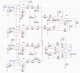
Can someone check if this is the proper way to use OPA1632 for balanced output of AK4499?
Any intentions with respect to balanced loads and build-out resistors for OPA1632?
I can tell you that what you are suggesting is rather different from what Topping did with D90. They used active summing of parallel dac channels with some brand of 49720 opamps configured for differential summing only (no filtering). They then produced the unbalanced RCA outputs by differential summing of the summed-channel balanced outputs.
I'm trying to follow what the eval board schematics and datasheet suggest, but with the addition of OPA1632 for balanced outputs. This works in simulator. I just asked if more knowledgeable folks would comment on possible mistakes/improvements.
Any intentions with respect to balanced loads and build-out resistors for OPA1632?
I can tell you that what you are suggesting is rather different from what Topping did with D90. They used active summing of parallel dac channels with some brand of 49720 opamps configured for differential summing only (no filtering). They then produced the unbalanced RCA outputs by differential summing of the summed-channel balanced outputs.
Mark,
can you post schematic of that output stage
Any intentions with respect to balanced loads and build-out resistors for OPA1632?
I can tell you that what you are suggesting is rather different from what Topping did with D90. They used active summing of parallel dac channels with some brand of 49720 opamps configured for differential summing only (no filtering). They then produced the unbalanced RCA outputs by differential summing of the summed-channel balanced outputs.
Yes, there should be output resistors of say 22-100 Ohms after OPA1632.
Mark,
can you post schematic of that output stage
Maybe I could post some of it, but you should understand that the output stage is pretty perfunctory. The AK4499 datasheet suggested I/V works fine if the physical implementation is good. However, a possible problem is that the suggested passive filtering of the I/V stages does not fully filter out some RF at twice the BCLK frequency (and some other lower level stuff). IME the RF can cause some low level yet slightly audible distortion in downstream equipment.
In any case, the output stage is only one part of a good AK4499 implementation. Other things need to be 'right' too. Clocking and I2S data jitter also affect sound quality (I2SoverUSB is not quite good enough to get the best out of the dac).
The 8 dac chip output channel voltage regulators can affect the sound significantly.
If the dac output channels are paired up then the number of output voltage regulators can be reduced to 4. They still should be chosen for best sound quality.
Topping did not use RF LDOs for that, although they did use LDOs recommended for dacs, but with only 0.5v drop across them. The input voltage for those LDOs is provided by two of some brand of SMD 317 type linear regulators.
The power supply voltage for the I/V opamps also affects sound quality, as does the peak digital input level going into the dac.
There are many details to optimize for AK4499 to sound as good as it can.
So, to my way of thinking and in the context of today's discussion, whether or not one chooses to use OPA1632 for balanced outputs is kind of a small thing in the big picture. May depend in part how it responds to low level RF over the BCLK x2 frequency range for sample rates the dac may be used at. The opamp datasheet might not show possible sensitivity as well as prototype testing could.
What I would suggest for you samoloko would be to build the I/V circuits and differential summing circuits suggested in the AK4499 datasheet. No need to parallel channels too early in the development process, its not needed for the dac to sound great. Its all the other things that matter more.
- Home
- Source & Line
- Digital Line Level
- AK4499 DAC Design