One could try 7SB3257.
Or maybe something like: https://www.analog.com/media/en/technical-documentation/data-sheets/ADG3248.pdf
Haven't really studied the datasheet yet, but anyone is free to do so 🙂
Also, could be Chris719 or someone else around here already has some experience with the bus mux/demux switch device applications. Haven't used them before myself.
Hmm....With some more reading looks like this type of device clamps voltage (according to ADG3248 datasheet) :
3.3 V to 2.5 V Translation
When VCC is 3.3 V and the input signal range is 0 V to VCC, the
maximum output signal is clamped to within a voltage threshold
below the VCC supply.
In this case, the output is limited to 2.5 V, as shown in Figure 22.
This device can be used for translation from 2.5 V to 3.3 V
devices and also between two 3.3 V devices.
Last edited:
since this is neither cheap nor easy device, why not go with some solution that doesnt require fiddling around pcb after device is assembled and closed. please someone check is 7SB3257 applicable here, or recomend part that could be used, also it would realy be nice to switch clock source via simple button press.
or make 2 different pcbs one with clock routed to connector and no xtal on board, and one with clock and no connector. please advise.
Use an RF relay if needed to get the desired isolation. An Axicom HF3 S gives 95 dB @ 100 MHz. You won't get that from a single CMOS switch or buffer. I would guess 7SB3257 is old because it's specified at 4-5V mostly.
Thanks Chris, but looks like Newark carries that part for about $23.
The non-shielded version (HF3) should be cheaper and nearly as good. Even a standard relay should be fine if you’re able to tri-state or turn off the other clock.
also it would realy be nice to switch clock source via simple button press.

that is not realy helpful, do recomend better solution, do tell why not do something, do explain in detail how all should be connected and used so it is not useless...
but i am starting to think this is wasting my time and i will learn absolutely nothing from this, for starters why do src need switching clock source at all, why not use datasheet recomended and be done with it? also why not use ak4137 slave mode for clock input, is it different kind of clock. please explain ...
also is preregulator with enable function and bunch of small regulators on all needed supply pins overkill?
Attachments
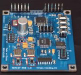
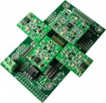
Attached below is a pic of a cheap Chinese AK4137 board. The red boxes show were some voltage regulators are. As can be seen, there is one for each clock, a big one behind the big filter cap, and another one kind of in the middle I would have to check to see what it is powering. The board sells for about $30 including shipping.
That's a piece of cheap junk, one might say, and now we have complaining about doing something maybe a bit better?
Nobody is forcing anyone to do anything they don't want to do 🙂
EDIT: By the way I used one of the boards below in the design of my 2nd modded ES9038Q2M dac. Removed the 22.5Mhz clock and brought in an external 25Mhz clock derived from dividing the dac clock by 4 using LMK01000 which required conversion to LVDS and back again. Lots of work, didn't let it stop me.
Attachments
Last edited:
do you think i am complaining for doing something better while it is clear from my posts that i dont even know difference of what is better or worse and asking for help?
could you please talk in non native english speakers friendly way.. some simplified non sarcastic, straight version?
without straight answer in this form; external clock is needed for (insert why) , and it should be swtchable because (insert why), and regulating everything is (insert good/bad) because (insert why); i dont understand what you want to say with that china pcb.
if making stuff even more complicated than it realy is, is all here will be and i will not learn something from this of course i dont see a point in wasting time here.
Sorry things are not clear. To my understanding, it has not been decided yet what the overall clocking scheme will be for the dac project. For simplicity and low cost, I would suggest that AK4137 should simply receive one external reference clock signal, and no other clock source should be needed.
Optionally, if one wanted to make the AK4137 board more generally useful, say, for other projects, it wouldn't hurt to provide pads for a clock, voltage regulator parts for it, and a jumper to select it (possibly including the ability to turn of its voltage regulator when it is not in use). That sort of thing could be completely optional, up to whoever wants to design an AK4137 module I guess. Reason for saying I guess is we still don't have a perfectly clear idea of how the project is envisioned to be divided up in modular fashion.
An overall system concept block diagram and some interconnection standards for how things will plug/solder/wire together could be useful, seems to me anyway.
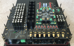
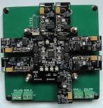
Some examples of other people's ideas below.
Optionally, if one wanted to make the AK4137 board more generally useful, say, for other projects, it wouldn't hurt to provide pads for a clock, voltage regulator parts for it, and a jumper to select it (possibly including the ability to turn of its voltage regulator when it is not in use). That sort of thing could be completely optional, up to whoever wants to design an AK4137 module I guess. Reason for saying I guess is we still don't have a perfectly clear idea of how the project is envisioned to be divided up in modular fashion.
An overall system concept block diagram and some interconnection standards for how things will plug/solder/wire together could be useful, seems to me anyway.
Some examples of other people's ideas below.
Attachments
Last edited:
that is not really helpful,
That may well be so but you made the suggestion. Do you not think the first person who should be able to answer the question 'why' should be you ?
thanks , that actualy helps a lot.
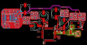
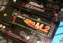
that is bit weird looking, i was thinking more with lets say m.2 slots of different sizes with different parts of circuit that you can screw securely to "motherboard" that has main regulation and routing on it so it would be universal to change different critical parts, and was under impresion that m.2 slot would be fine for high freq signal if neighbouring traces were grounded. also have never checked would fattening on m.2 slot be possible or would it have enough pins to satisfiy all needs, see attached picture.
@rfbrw, i made suggestion using chip in place of pins, but have never known purpose of changing at all, why would i go trough hassle of finding part, reading datasheet, making footprint, puting it onto pcb, only to remove it now as it is actualy not needed and simple gold plated pins are good for that use. also again not helping at all.
Attachments
Are saying you made the suggestion as to changing clocks without actually knowing why you are changing clocks ?
exactly. i am still not sure why would one prefer to take clock from somewhere else while in same time having clock directly there where it is needed, please explain if you have time/will.
toni, the m2 slot is along the lines of what i was thinking, I was also considering PCIe, but you’re definitely thinking along the same lines as me. I think using pci cards might also let me use part of a pc chassis as a test bench for the project before making the final chassis.
exactly. i am still not sure why would one prefer to take clock from somewhere else while in same time having clock directly there...
The AK4499 eval board does exactly that, it gives users the ability to use a MCLK signal generated by AK4118 SPDIF receiver so that incoming SPDIF does not have to be resampled by AK4137. It also allows for clocking AK4137 from AK4118 if upsampling is desired to be in sync with the SPDIF recovered clocking.
The best option IMHO in most cases, if not all, is to use AK4137 with a local crystal clock, ideally one located next to the dac chip. At least users can see for themselves if including AK4137 in their own design would be worth the cost and added complexity.
Maybe someone else will think of other use cases. If only doing clock switching for some one-time comparisons I don't see why jumpers would not be sufficient. If someone has other ideas, maybe they will speak up.
Last edited:
The AK4499 eval board does exactly that, it gives users the ability to use a MCLK signal generated by AK4118 ......
Sorry, I have not followed this thread really, but are you implementing external only MCLK here?
...are you implementing external only MCLK here?
Don't think so for the dac board itself. Last few posts were about clocking an AK4137 ASRC.
Beginning on defining a system-level design: Thinking of having a main board with very minimal circuitry, actually just the power switch, a power supply for an 8V bus, and the serial isolation circuitry. Given the relatively complex power-up sequence for all the chips onboard, I'm also thinking of putting an i2c controlled PMIC from TI, which will also give metrics on the dac rails, maybe even some current measurements, which may be useful for debugging. I still have some figuring out to do with where I want to put the clocks, more info on that to come soon. I then want to have .1" pitch headers to mount a microcontroller board, this is not a critical or high-speed interface so these should be okay, I also plan on integrating screen control circuitry on the microcontroller board, so plan on including a connector for the screen on the board near the microcontroller. I then want to have likely the following solution, unless anybody has any better recommendations: Individual PCIe cards for the input, ASRC, and DAC chips, with SMA connectors in between them for time-critical signals. Planning on separating DAC and I/V stage into two sub-boards on the same card, clocks will either be on one of the cards or on a seperate card feeding each of the other cards. Probably going to keep jumpers to switch between clocks, can't imagine a time when I would need to switch clocks other than during testing, where the chassis will be open anyway.
PCIe extenders and longer SMA cables for troubleshooting and or measurements?
Also, boards can be too close together if EMI fields can interact too much in a parallel geometry. Already have observed audible issues with too-close-coupling using JLSounds I2SoverUSB and AK4137 boards with AK4499 eval board. Have seen similar/worse issues in RPI hat DAC stacks. Shielding can help a lot, but tends to get in the way of development and or experimentation activities.
Also, boards can be too close together if EMI fields can interact too much in a parallel geometry. Already have observed audible issues with too-close-coupling using JLSounds I2SoverUSB and AK4137 boards with AK4499 eval board. Have seen similar/worse issues in RPI hat DAC stacks. Shielding can help a lot, but tends to get in the way of development and or experimentation activities.
Last edited:
- Home
- Source & Line
- Digital Line Level
- AK4499 DAC Design