I’d prefer to just run the clock over the board to board connectors if they are designed for high speed use, which a PCIe connector is.
If you are worried about EMI, you can always provision the boards for a shield and you can also bury traces between stitched planes where appropriate.
In general I am not a fan of over-modularizing things except for prototyping. I find that it helps to narrow the scope instead of trying to accommodate every possibility.
Concern about running clocks though a back plane is steps need to be taken to assure signal integrity if the clock is distributed to multiple devices in parallel. That is a type of design not typically encountered in dacs where we are trying to keep clock signals perfect. The connector itself doesn't bother me if it is made for high speed use and proven very reliable. (I don't put u.fl connectors in that class as durability is not very good, IMHO.)
Agree with Chris about not over-modularizing if possible.
Agree with Chris about not over-modularizing if possible.
Last edited:
toni - What’s up with all those pins? On the backplane, all the lines will be shared so need to take into account which pins for which cards, and i’ll be using I2C control so i suspect most of those are unnecessary.
Been thinking about this project a bit more, figure there's no point in including all of the indivudual voltage regulators from the eval sheet, I think I'm at a point now where I feel comfortable diverging. I just wanted to get far enough that I felt I understood the choices being made on the eval board, and I am now at that point. See the PDF linked in other pages for the "final" version of the eval board schematic. Next steps are defining the PCIe connector interface, I plan on using a 4x slot with SMA connectors for clock and I2S signals. I plan on putting the input connectors on the same card as the AK4118 DIR chip, having another card for the SRC, and a third for the DAC and I/V stage. Debating putting output connectors on the backplane or on the card, it would increase the width of the card past the PCIe specification, making it virtually impossible to use an old PC chassis as a test bench, like I was planning to do, without cutting out one of the slots to be double width. Looking for some feedback around this, how you guys would do it if it were up to you. I plan on getting some schematics, documents, specifications, etc. onto github in the coming days to open it up to input from the community.
Also, looking at the PCIe specification, I see 12V lines, obviously should have no problems running 8V over these, but what about 15V? Figure it shouldn't really be a problem, as a connector is a connector, but wondering if I should put another connector on the I/V stage card and run a cable directly from the backplane.
Also, looking at the PCIe specification, I see 12V lines, obviously should have no problems running 8V over these, but what about 15V? Figure it shouldn't really be a problem, as a connector is a connector, but wondering if I should put another connector on the I/V stage card and run a cable directly from the backplane.
Last edited:
...figure there's no point in including all of the indivudual voltage regulators from the eval sheet...
Does that apply to the Jungs and the NJM7805s?
Mark, didn't mean not including them on the final design, just meant not including them in this version of the schematic. All the regulators from the eval board will either be included or replaced on the final version, just didn't want to create all those kicad parts that will just end up being changed between boards.
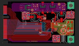
Wondering if anybody has any resources apart from the datasheets that may be useful in doing layout of this DAC board, specifically the higher speed signals and grounding considerations.
Adam,
You really should take a look at Ott's book, the bible for that sort of thing: https://www.amazon.com/Electromagne...77PX784K3XA&psc=1&refRID=7CDE30Q3977PX784K3XA ...tons of very practical information. Don't let the title make you think it isn't what you need.
Another great one that should be in your reference library: https://www.amazon.com/High-Speed-D...69C5M06W4YQ&psc=1&refRID=MYHXTR23Q69C5M06W4YQ ...lots about clocks and clock signal distribution among other things.
Last edited:
hello adam,
sort of been following along, i have glossed over akd4497-sa document
i see they are using source series termination for most of the high speed signals, so I assume one would run 50 ohm transmission lines. For that you need to determine your stack up and trace widths.
I did some high speed designs, now many years ago but there were a few Intel documents on high speed layout, specific to the serdes chips we were using. Also some others too I 'd have to look, its been a while. We were running GHz signals so via design was critical. Have to concern yourself with stubs.
We also used a s/w tool called hyperlynx used for modeling our signals, that and IBIS models of device I/O's. We were using high end pcb layout tools, it was a luxury but these designs can be done if basic rules and techniques are followed.
In a nut shell there are general rules to follow like having a continuous ref plane, controlling the Z using a strip lines or microstrips. Via design. Now that I think about it, way back we referenced a Motorola ECL handbook, authored by a guy by the name of Blood iirc, I think I have it in my disk, have to look. Onsemi still makes ECL logic so that is a good place to look for high speed design info, that and some pcb mfgs have info as well. I will look at what i have, maybe I'll put them up on my google drive for you to review. okay that is what I'll do and provide you with a link.
Google Drive: Sign-in
Enjoy, just bit of light reading 🙂
As a suggestion, create a Google drive to put up your documents so I can review them. Collaboration of a design in a forum like this can have its challenges because it can be a PITA to find info, esp when people go off topic.
best i can do for now
Rick
Last edited:
A good resource for high speed pcb design
Douglas Brooks Articles on PCB traces, temperatures, and signal integrity
Douglas Brooks Articles on PCB traces, temperatures, and signal integrity
Rick -- Thanks so much for the adviceI was planning on putting all relevant documents up on github, if there's a preference for google drive, I can also put it there, but I've grown up on git so am quite comfortable with it, and it should make it easier to track tasks / issues / collaborate. The one thing I'm worried about is posting copyrighted material (Books, eval board datasheets, etc. on a public forum, thoughts on this matter? I do like the idea of centralizing documentation / schematics / layout to facilitate collaboration and keep this thread on-topic. I am starting college soon though, so will likely not have as much time as I would wish to keep working on this over the next couple weeks.
Also, I have no problem finding books, but I am wondering what free software resources are available, especially on macOS / linux (until I get bootcamp set up) for signal integrity simulation / analysis. I stumbled upon eispice a couple days ago, and will probably use that, but was wondering if others had any recommendations.
Also, I have no problem finding books, but I am wondering what free software resources are available, especially on macOS / linux (until I get bootcamp set up) for signal integrity simulation / analysis. I stumbled upon eispice a couple days ago, and will probably use that, but was wondering if others had any recommendations.
Last edited:
Here is the link to the github repository that I will be using for this project, I added some documentation, planning on adding my parts libraries and schematics later today.
Also, rick, just managed to track down the motorola ECL handbook, on my phone now but will upload to git later.
GitHub - tobycyanide/AKDAC: An OSHW design for an AK4499 DAC
Also, rick, just managed to track down the motorola ECL handbook, on my phone now but will upload to git later.
GitHub - tobycyanide/AKDAC: An OSHW design for an AK4499 DAC
Last edited:
Also, I have no problem finding books, but I am wondering what free software resources are available, especially on macOS / linux (until I get bootcamp set up) for signal integrity simulation / analysis. I stumbled upon eispice a couple days ago, and will probably use that, but was wondering if others had any recommendations.
HyperLynx
Hi Adam,
I only use Microsoft these days so I am not aware of MacOS or Linux s/w.
Your design IP you have to consider if you want it shared but you did say you wanted to do a open design so can't have it both ways.
If you do not want to post copyrighted material, then just put a link to it instead.
Thanks for the github links, might work better in fact for collaboration.
Good luck with College, maybe the prof's can help you out with this design. Nothing like making practical out of theory 🙂
Cheers Rick
i am confused I2C spec has max freq stated 5MHz, clock is at 26MHz, at 0.16mm height and 0.25mm trace thickness that is aprox, 52Ohms.
why do we need special connector for I2C(S) while pcie spec is routing multiple even faster signals trough connector? are those differential or what but it should work good for this use.
it is hard to conclude what is needed and what is too much.
also would it be better to pass singal trough few vias and route it in middle layer sandwitched or two middle layers ground while top and bottom signals?
what is with vias dimensions on high speed, what are rules?
also thinking of single board simplified solution more and more, at least as side project, all this connectors are good for prototyping but for end product it seems more complicated altough it will be nice to have modular device that people can diy their own cheap pcbs and make it piece by piece..
...do we need special connector for I2C(S)?
No special connectors needed for I2C.
I2S and MCLK are the digital signals we want to keep in good shape, especially so for MCLK. Mostly the concern about things like: jitter introduced by poor connector contacts, ground bounce issues, potential cross-talk, etc.
Regarding source terminated 50-ohm transmission lines recently mentioned by someone, they are not commonly needed for dac I2S signals since the signal runs are normally kept pretty short. In addition, we want to preserve logic levels at the receiving end. At least some dac chips are clearly specified for normal logic level input signals.
Although the AK4499 evaluation board schematic shows 50-ohm resistors in series with the I2S and MCLK lines, they are not located at the source end. Rather they are located somewhere roughly in the middle of the lines as damping resistors for non-impedance-controlled interconnections.
The idea with the modularity is to have this design as easy to iterate on as possible, maybe once it’s “finalized” a single board solution would be preferable. I’d like to be able to swap out any individual module without having to get the whole board remade, and the modularity lends itself well to a relatively small form factor IMO because of the stacked boards. Yes the connectors will add expense, but it should only be a one time cost with the advantage lasting the lifetime of the DAC. Also, I plan on releasing the source files for this project under CC-BY-NC or CC-BY-NC-SA, any thoughts on either of those?
- Home
- Source & Line
- Digital Line Level
- AK4499 DAC Design