Scope probes - 10x vs 1x?
Hi guys. I've been away for the last week or so and haven't been able to play with this at all until today.
I have a question about correct scope use - the Rigol manual is useless in this regard. My scope probes have a 1x vs 10x switch. I have always been using 10x together with 10x in the Channel probe setting on the scope, thinking these merely had to match and 10x must be better than 1x. 😱
Today I tried 1x at the probe and 1x in the Channel probe setting. I wasn't expecting such a dramatic difference in results which are presented below. Perhaps the differences are also informative and, more to the point, perhaps I am using my scope improperly (or perhaps it has issues).
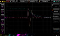
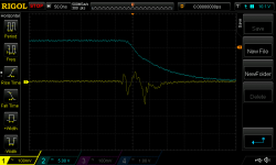
Turquoise trace = gate voltage on chop chop box pass transistor
Yellow trace = Vout of regulator
Blue trace = ground of regulator near the op amp
(All probe GND alligator clips connected to chop chop box GND A pin.)
I read this document which discusses 1x vs 10x probes and recommends using a properly adjusted 10x probe because the capacitance in the probe is reduced by a factor of 10 leading to less ringing potential in the probe itself.
However, having read this, I was still expecting to see generally the same waveforms in my scope in either case except potentially less ringing when using 10x. I see the opposite with respect to ringing, very different amplitude differences and I don't understand why the gate voltage waveform is slower to rise in the 1x case.
User error?
Hi guys. I've been away for the last week or so and haven't been able to play with this at all until today.
I have a question about correct scope use - the Rigol manual is useless in this regard. My scope probes have a 1x vs 10x switch. I have always been using 10x together with 10x in the Channel probe setting on the scope, thinking these merely had to match and 10x must be better than 1x. 😱
Today I tried 1x at the probe and 1x in the Channel probe setting. I wasn't expecting such a dramatic difference in results which are presented below. Perhaps the differences are also informative and, more to the point, perhaps I am using my scope improperly (or perhaps it has issues).
Turquoise trace = gate voltage on chop chop box pass transistor
Yellow trace = Vout of regulator
Blue trace = ground of regulator near the op amp
(All probe GND alligator clips connected to chop chop box GND A pin.)
I read this document which discusses 1x vs 10x probes and recommends using a properly adjusted 10x probe because the capacitance in the probe is reduced by a factor of 10 leading to less ringing potential in the probe itself.
However, having read this, I was still expecting to see generally the same waveforms in my scope in either case except potentially less ringing when using 10x. I see the opposite with respect to ringing, very different amplitude differences and I don't understand why the gate voltage waveform is slower to rise in the 1x case.
User error?
Attachments


As in the probe compensation? No.
I had not gone through this at all (until now). I was told the scope was calibrated by the supplier - part of their sales pitch.
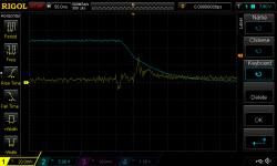
I just now went through the probe compensation process for each probe. All looked pretty good for both 1x and 10x settings on the probes themselves. I made very - and I mean very - minor changes for 10x on a couple of the probes. These were really fussy changes. In general the square wave responses were very good (in comparison to the guidance for over- under-compensation given in the manual).
I had not gone through this at all (until now). I was told the scope was calibrated by the supplier - part of their sales pitch.
I just now went through the probe compensation process for each probe. All looked pretty good for both 1x and 10x settings on the probes themselves. I made very - and I mean very - minor changes for 10x on a couple of the probes. These were really fussy changes. In general the square wave responses were very good (in comparison to the guidance for over- under-compensation given in the manual).
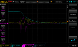
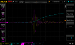
The "Chop Chop Box GND A vs Reg Vout" (yellow, 10x) and the "Chop Chop Box GND A vs Reg GND at output" (magenta, 10x) waveforms are remarkably similar. Here I shifted to the trailing edge of the gate voltage waveform. Pic 1.
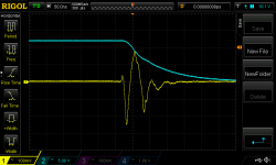
So next I moved both GND alligator clips from Chop Chop Box GND A to the GND pin at the output of the regulator (near where I am probing Vout). Pic 2. Note the change in scale for Vout (yellow) - quite a difference.
So next I moved both GND alligator clips from Chop Chop Box GND A to the GND pin at the output of the regulator (near where I am probing Vout). Pic 2. Note the change in scale for Vout (yellow) - quite a difference.
Attachments
10x is usually used because it has less effect on the circuit.
1x is used when one needs the extra sensitivity.
But 1x does very significantly reduce the frequency response of the probe+scope.
I read recently that a piece of 50ohm coax is a far better 1x probe. This apparently maintains the coax+scope frequency response.
I have used this with some BNC T piece connectors to feed the test signal into the DUT and into the scope simultaneously. Works flawlessly.
Jan is suggesting that you connect your probes to a known-good square wave generator with fast risetime and no overshoot (such as the Compensation Signal available at the bottom right of a Rigol DS2000 scope). Then twirl and dial the trimmers inside the probe body until you get the best looking square wave. Do this for each probe. The Rigol manual says more.
Do this every time you change from 1X to 10X so you're always using known-good probe compensation at that attenuation.It has nothing to do with the scope mainframe box which indeed is tested and calibrated in the factory. It has everything to do with the individual probes, which require different compensator settings on 1X than they do on 10X.
You could also fool with the Bandwidth Limit option. It will remove some of the zippety zing from your displayed waveforms. But is this what you actually want?
_
Attachments
I understand and will start such good practice from now on. Thanks for the links.
The point I made, though, in #643 was that when I did look at the probe compensation (as per the manual) the square waves were very good for both 1x and 10x use. I only made a very, very slight adjustment to two of the probes. (In one case I wanted to see what under- and over compensation looked like. So I adjusted the probe and then dialled it back to square.)
So I am still puzzled by what I see in #641. Perhaps it is as a result of reduced frequency response from 1x... I will just stick to 10x use.
Any thoughts on #644?
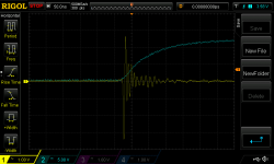
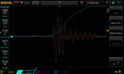
644 pic2 is what you have been wanting to see for 5 weeks. It is here, hallelujah. The only mystery is why the gate node in blue, doesn't show the ringing. Since blue is generated by a 6 ampere driver whose ground is 641 pic1, I expect it to follow the ringing ground.
Maybe now is the time to view the voltage waveform at groundpoint X using a probe whose grounding_clip is on groundpoint Y, and vice versa.
Maybe now is the time to view the voltage waveform at groundpoint X using a probe whose grounding_clip is on groundpoint Y, and vice versa.
I'm not quite jumping for joy, but it does seem more encouraging... I'm wary of falling into a sort of circular situation where the improvement is just optical because I changed the way I conducted the observation.
Just in case I wasn't clear the blue trace in Pic 2 has the probe ground clip at the reg output GND pin (alongside that for the probe checking Vout). What's disappointing to me is that this isn't much closer to GND A on the Chop Chop Box.
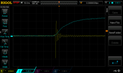
GND A is definitely the quietest with respect to the regulator GND pin (at the output) of all the GND probe points on the Chop Chop Box. In the below pics the yellow trace alligator clip is at reg output GND pin versus the probe at (a) Chop Chop Box GND A, (b) the base of the Chop Chop Box fasten connector and (c) reg output GND pin i.e. at its own alligator clip. Working backwards, I take from (c) that some of this is probe inductance related. I presume (b) is the cumulative effect of probe inductance and the short wires connecting the chop chop box. The difference between (a) and (b) seems odd to me - the difference in probe point is just a few millimetres of thick copper traces and solder-soaked braid.
As to the blue trace not following the ringing ground, it would be challenged to show up with 5V per division (DC coupling). The last pic is a closer look at the gate voltage waveform (leading edge as it is easier to see the issue). Blue is with the alligator clip at Chop Chop Box GND A; yellow is with the clip at the regulator GND pin at its output..... Just need to connect the remaining dots after some sleep. I wonder if I didn't make a mistake in the way I laid out the grounding on the chop chop box (i.e. a better path for the discharging to ground of the gate capacitance by the MCP1407 through to fasten ground connection or similar issue).
Since blue is generated by a 6 ampere driver whose ground is 641 pic1, I expect it to follow the ringing ground.
Just in case I wasn't clear the blue trace in Pic 2 has the probe ground clip at the reg output GND pin (alongside that for the probe checking Vout). What's disappointing to me is that this isn't much closer to GND A on the Chop Chop Box.
GND A is definitely the quietest with respect to the regulator GND pin (at the output) of all the GND probe points on the Chop Chop Box. In the below pics the yellow trace alligator clip is at reg output GND pin versus the probe at (a) Chop Chop Box GND A, (b) the base of the Chop Chop Box fasten connector and (c) reg output GND pin i.e. at its own alligator clip. Working backwards, I take from (c) that some of this is probe inductance related. I presume (b) is the cumulative effect of probe inductance and the short wires connecting the chop chop box. The difference between (a) and (b) seems odd to me - the difference in probe point is just a few millimetres of thick copper traces and solder-soaked braid.
As to the blue trace not following the ringing ground, it would be challenged to show up with 5V per division (DC coupling). The last pic is a closer look at the gate voltage waveform (leading edge as it is easier to see the issue). Blue is with the alligator clip at Chop Chop Box GND A; yellow is with the clip at the regulator GND pin at its output..... Just need to connect the remaining dots after some sleep. I wonder if I didn't make a mistake in the way I laid out the grounding on the chop chop box (i.e. a better path for the discharging to ground of the gate capacitance by the MCP1407 through to fasten ground connection or similar issue).
Attachments
Last edited:
You need to get into the habit of hand-drawing a schematic showing the PSU board (as a box), the ChopBox (as a box), the inductive load resistor, the six wires which interconnect these, the two scope ground clips, and the two scope probe tips.
You know how these are configured. Your readers don't.
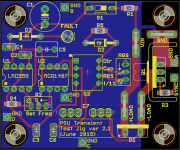
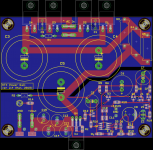
Chop chop box board and PSU board for reference. GND points labelled on the former (GND A is located on right side of board). References to "reg output GND pin" refer to the pin on the regulator board located near the output fasten connectors (bottom left). Reg Vout is being probed at the pin near the Vout output fasten connector.
Attachments
Last edited:
Shifting all the probe alligator GND clips from Chop Chop Box GND A to the reg output GND pin produced an aesthetically pleasing result when looking at the trailing edge of the gate waveform stimulus. #644 pic 2. However, as I had feared, the issues appear to just be masked.
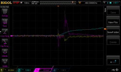
Pic 1 , to which I have added the magenta trace which probes GND A with respect to the reg output GND pin, seems to indicate the swings in the relative GNDs remains a factor/indicator.
Things are more evident when looking at the leading edge of the gate waveform. Pic 2 has the GND clips stacked on GND A, pic 3 with them stacked on the reg output GND pin. Similar but less amplitude for the latter. The last few pics add the same relative GND trace (magenta) as mentioned above. The relative GND trace seems to move almost perfectly inverse - at least at the beginning - to the Vout trace (yellow), albeit with greater amplitude (note different scales). Note also, the uneven rise in the blue trace.
This all still feels like a bit of a crap shoot... 🙂
Attachments

Apologies to Jan - the technique you introduced for comment is way above my experience level; perhaps Mark and others will provide their views (either here or directly).
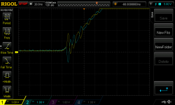
FWIW, with the Chop Chop Box gate stopper resistor Rgs engaged to slow the stimulus rise time. I measure 294 Ohms for Rgs as dialled with my multimeter. Much less than this and I start to get the patterns above. (Same setup as above - all probe GND clips at reg output, yellow trace is Vout at reg, magenta is probing GND A on the Box.)
I'm going to order the revised PSU boards and then build the 5V and 3V3. I may as well, even if the entire thing ends up in the bin! In the interim, if anyone has any bright ideas regarding this transient testing I'd love to hear them. 😀
I'm going to order the revised PSU boards and then build the 5V and 3V3. I may as well, even if the entire thing ends up in the bin! In the interim, if anyone has any bright ideas regarding this transient testing I'd love to hear them. 😀
Attachments
Apologies to Jan - the technique you introduced for comment is way above my experience level; perhaps Mark and others will provide their views (either here or directly).
? Which one?
I'm going to order the revised PSU boards and then build the 5V and 3V3.
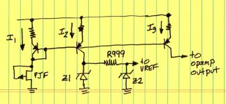
I suggest you do two things before ordering parts: (i) recalculate the value of resistor R999; (ii) seriously consider ordering at least 25 pieces of MMBFJ175.
Your three legged current mirror is shown below; the currents in the three legs are equal. The current is set by the IDSS of Pchannel JFET "PJF". I1 = I2 = I3 = IDSS(PJF).
You are in a box. You can't set the current too high and you can't set the current too low.
If you set the current too high, then I3 will exceed the available output current of your opamp. Remember that your opamp MIGHT be a TL071 or other device whose output current is about 20 mA.
If you set the current too low, then you won't be able to overcome resistor R999. (The current in R999 equals (VZ1 - VZ2)/R999). I'd suggest at least 4mA in zener Z1 and another 4mA in R999+Z2.
So you need an R999 big enough to drop (VZ1 - VZ2) with a current of only 4mA.
And you need a Pchannel JFET whose IDSS is between 8mA and 19.9mA.
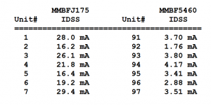
Fortunately, it's pretty easy to measure IDSS of a surface mount JFET using a 9V battery, a DMM set to milliamps, and three microhooks. Also fortunately, they all have the same pinout. So I measured seven units of your current device (MMBF5460) and seven units of a possible replacement (MMBFJ175). Data is below.
Or you could just replace the PJF with a resistor and get slightly lower attenuation of input ripple fed through to VREF.
_
Attachments
Hi. Thanks. I purchased parts for all three voltage rails at the same time. But a few more JFETs and resistors won't be an issue.
The revised version of the board entrenches the powering of Vref and the op amp from Vout. The current mirror simplifies as your I2 and Z1 are removed (and 12Vout feeds your "R999"). In the case of the 5V and 3V3 rails, they're powered from 12Vout whether I use the current boards or the revised one and the current mirror etc isn't populated in either such case.
I could use the existing boards for 5V and 3V3 as originally intended. However, the currently populated 12V board has taken a real battering. Ideally I'd populate a new board (the only significant cost is the main filter caps as I doubt I could recover them from the existing board - they had adhesive bases). I was thinking that if I commit to a Vout driven typology for 12V I may as well tidy up the jerry-rigging for the 12V rail into a new board layout (as well as clean up the error I made with the voltage stepper pin layout and a few other nits to make soldering easier etc) and use this for 5V and 3V3 as well. I'm still on the fence a bit but £30 buys me 'neat and tidy'.
Nonetheless, in any case, your points regarding the current mirror for the 12V rail make sense. I'm hoping to find a supplier of the clips that doesn't charge £12 delivery but if I had to pay that then so be it.
In the jerry-rigged 'Vout-driven' board I have been testing, Z1 is removed and 12V from Vout is fed (via an added wire from C12+ to R15) through two 499R resistors in series (R15 and R10) to power the LM329 Z2. I realise I have the LM329 current towards the upper end of its recommended operating range.
Attachments


Last edited:
I realise I have the LM329 current towards the upper end of its recommended operating range.
Oops! No it's not. (c5.5mA)
I take it you remain a strong proponent of not powering the op amp and Vref from Vout even when the witnessed ringing seems to be a test issue i.e. probing Vref shows a similar waveform even though C8 (now 220uF) suggests it can't be the case. How much shelter do the op amp bypass caps C10 (0.1uF MLCC) and C11 (4.7uF tantalum) provide the op amp (while R11 and C8 shelter Vref)?
(Part references are those in the schematic in the previous post.)
Last edited:
Naaah, connect the opamp and Vref however you like; it's your circuit and your design. I did not know you had made the final decision, I had been assuming the modifications were expedient but temporary kludges.
- Status
- Not open for further replies.
- Home
- Amplifiers
- Power Supplies
- Adventures with 5A regulated voltage circuits