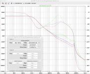
Hi Andrew. If you hover your mouse over a thumbnail you can see the filename. Left is Vin and right is Vout.
Ah, better stability margins using Vin as power supply.
To be expected.
I clicked on each to see what was to be seen, then I get no confirmation of what each title is.
To be expected.
I clicked on each to see what was to be seen, then I get no confirmation of what each title is.
An element of progress. I fitted the two zener diodes across gate
You only need one zener of course.
Jan
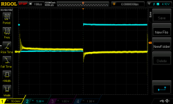
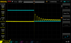
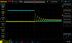
Well it is nice to get to testing without flames, but the results don't look good. Here's a series of scope pics when switching from no load to an 8 Ohm load and back. The first three look at the load coming on, with increasing zoom, and the last three the load coming off.
This is with a 100p/47R Zobel from drain to gate rather than a gatestopper resistor (R12). There's no compensation network around the op amp. The modelled phase margin of this setup is the left pic in post 479.
I'm a bit unsure whether to drop the Zobel for a gatestopper or try to add compensation around the op amp with the Zobel in place. Hmmm....
Attachments
Last edited:
Now is the time to issue your second plea for attention, to diyAudio members peufeu and Elvee. You can impress them with your expertise by remarking that of course the oscillation is worse when output current steps down from (big current value) to (small current value) since that immediately reduces the gm of the pass transistor, just when you need it to do something dynamic.
Ok.
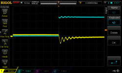
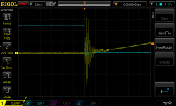
I recalled that Cy of 47p was left in place and so decided to solder back in a 0 Ohm jumper into Ry and test the impact of adding compensation around the op amp. My LTspice model suggests that this reduces the unity gain frequency from 4.5MHz (phase margin of 180-91.5=88.5 degrees) to 561kHz (phase margin increasing to 108.2 degrees). See attached.
To my eye there is no discernible difference in the waveform when the output current steps down and the first trough of the waveform when the output current steps up is slightly worse (although the general picture is relatively the same)!
Attachments

I think it is important to note that none of these psu's are meant, or designed, for sub-us load switching.
Without remote sensing you will always see this type of ringing in such cases, if only because of wiring induction.
It even makes a large difference where you measure on the wiring between psu and load, and how the feedback and grounding is arranged.
One more reasistic test: load the supply with say a 20kHz signal out of a power amp via 8 ohms and a series cap connected to the supply output.
Then see what residual you see at the supply output. You will be pleasently surprised! ;-)
Jan
Hi Jan. I will sleep on your comment. I just thought I would clarify that I am measuring the psu directly at the pads near the output caps (with probe and ground spring). There is, of course, a good deal of wiring from the output fasten connectors to my switch, chop-chop box and the attached power resistor and back again.
(I'm a bit reluctant to start using my Krell FPB power amp as a test device...😱)
I wonder if my Zobel strategy just isn't doing anything. I will test a 100 Ohm gatestopper given I've laid out my board to make it easy to do just that. Hopefully tomorrow...
(I'm a bit reluctant to start using my Krell FPB power amp as a test device...😱)
I wonder if my Zobel strategy just isn't doing anything. I will test a 100 Ohm gatestopper given I've laid out my board to make it easy to do just that. Hopefully tomorrow...
Phase margin likely less than 10 degrees judging from the number of bumps. But adding relatively significant compensation around the op amp makes no difference. Suggests the problem is elsewhere? Parasitic oscillation due to MOSFET internal capacitance? Hence I'm thinking I need to try the gate stopper resistor.
PS: the model is very insensitive to the values of Rz and Cz (the Zobel from gate to drain).
(As an aside, given how often these must be deployed in circuits and the high use of/need for modelling I would have expected manufacturer provided models to include/accommodate these sorts of things (by now). Looking inside the model for the IPP037N06L3G seems to indicate they have included the relevant capacitances. Anyhow....)
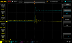
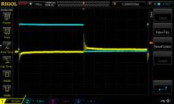
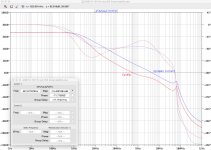
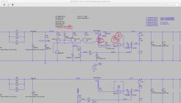
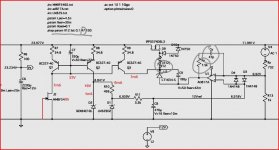
I did a quick test with the Zobel from gate to drain removed and a 47 Ohm gate stopper resistor inserted. The gate stopper scenario has additional compensation around the op amp of a series 47p cap and 7.5k resistor. See circuit extract. I have attached the modelled bode plot for this scenario (blue trace).
Again, there is little difference in the traces from those above (and the later test I did with the Zobel and compensation around the op amp; post 486). See attached (rising then falling).
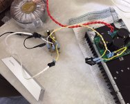
Jan, are you saying that any analysis is completely obscured by the effect of wiring inductance and so it is pointless to conduct this form of test? I attach also a quick pic of the test setup. Any suggestions appreciated.
EDIT: for those interested in digging into the LTspice models, I have attached these also.
Again, there is little difference in the traces from those above (and the later test I did with the Zobel and compensation around the op amp; post 486). See attached (rising then falling).
Jan, are you saying that any analysis is completely obscured by the effect of wiring inductance and so it is pointless to conduct this form of test? I attach also a quick pic of the test setup. Any suggestions appreciated.
EDIT: for those interested in digging into the LTspice models, I have attached these also.
Attachments

Last edited:
and got into trouble 😀I did a quick test
As you can see, the voltage on D2 is way to low.That's because the current from Q2 is used up through R10.
J2 has a Idss to small.Why a P-fet, with a very uncertain current ?
N-fets have less spread in current.Choose a 2N5485 with not the lowest current (=4mA
Mona
Attachments
Hi Mona
Have a look at posts 462 to 466. 😀
Yes, I could rebalance the current between the two Zeners with higher R10 or use a PFET with greater current e.g. MMBF5461 or switch to another construction e.g. NFET. It would help the quality of Vref, but there's little flow through to line rejection for the circuit as a whole. (What would make a very big difference is to drive the op amp and Vref from Vout.)
I think these are 'polishes' that can be tweaked later. For now I'm battling the broader issue of what I am seeing in transient testing. 🙁
Some remarks come to mind: why do you use such an insanely fast (50MHz) opamp?
Either you have to kill most of its bandwidth, or make sure that everything inside the loop behaves smoothly and predictably up to 50MHz+, and this includes the power part of the circuit. How can you control a few nH here and there, in the source of the MOS for instance?
The "zobel" on the MOS gate is essentially useless: it is simply connected between the opamp's output and a node equivalent to the ground in AC, it thus simply loads the output of the opamp, but other than that it has no effect
Hi Elvee, thanks for taking the time to chime in.
Regarding choice of op amps: see post 133 and 380.
Regarding the "Zobel" (100p cap and 47R resistor in series from drain to gate), the idea stemmed from a portion in Cordell's book which discussed it as an alternative to a gate stopper resistor. See post 188. The board circuit is in post 486 where you can see Cz/Rz and the gate stopper R12 (which is a 0R jumper if Cz and Rz are populated). But whether I use the 'Zobel' or a 47R gate stopper resistor I get the same output from my transient testing. (Posts 484 and 492.) (I guess if the 'Zobel' is doing nothing then I have simply tested the difference between no gate stopper resistor and a 47R one with added comp around the op amp....but even still....)
Is the test setup sensible?
Last edited:
As an aside for Jan...
In posts 210 and 215 Peufeu commented with respect to the use of remote sense and where to reference Vref to in such case. He made the comment that Vref needed to be referenced to Sense- and not the local reg board GND. It seems to me that the latest version of the schematic for the Jung/Didden regulator sold in the DIYAudio store shows Vref referenced to the reg board's local GND. Or am I mistaken?
In posts 210 and 215 Peufeu commented with respect to the use of remote sense and where to reference Vref to in such case. He made the comment that Vref needed to be referenced to Sense- and not the local reg board GND. It seems to me that the latest version of the schematic for the Jung/Didden regulator sold in the DIYAudio store shows Vref referenced to the reg board's local GND. Or am I mistaken?
As an aside for Jan...
In posts 210 and 215 Peufeu commented with respect to the use of remote sense and where to reference Vref to in such case. He made the comment that Vref needed to be referenced to Sense- and not the local reg board GND. It seems to me that the latest version of the schematic for the Jung/Didden regulator sold in the DIYAudio store shows Vref referenced to the reg board's local GND. Or am I mistaken?
Yes, I think it should be referenced to the sense. Time for V2.3 guess 😡
Edit: It really looks like I did that on purpose but I can't remember why....!
Jan
Last edited:
Okay so I am at a bit of a loss...
Are the scope shots above really merely showing me the impact of the trace inductance in the board, output caps and, much more significantly, wiring to and from the chop chop box and load resistor?
Is the latter completely obscuring any further analysis? I see the same thing on my scope screen even when I power the op amp and Vref from Vout.
Do I simply take some comfort that it didn't go completely unstable and move forward or do I have a real circuit problem (and perhaps should ditch the entire project!)?
I can model the circuit and see good phase margin, good transient response (except for the impact of output cap ESL) etc. But if I put it on the bench and can't see through the test setup wiring inductance I'm unsure what to do next.
Capacitance at the load should bear the brunt of any transient current needs...
I can tweak the board's output capacitance (smaller caps in parallel for better impedance profile, or even make any further iteration of the board use 2.5mm spacing output caps for lower ESL) but can only do this based on desktop modelling rather than observing the impact in the physical circuit. (Powering Vref and the op amp from Vout will provide a good deal of efficiency in any further board iteration as well.)
Argh...
- Status
- Not open for further replies.
- Home
- Amplifiers
- Power Supplies
- Adventures with 5A regulated voltage circuits