I am still bugged as to why a 2% voltage tolerance 10V zener (which had measured such previously) is reading closer to 9V...
Perhaps this may suggest a new angle from which to view the situation:
The 10V zener cathode is connected to the 6.9V ICzener cathode through a resistor (R10). How much current is flowing in R10? Ohm's Law says
- Current = Ir10 = (10V - 6.9V) / R10
But wait! What if the PJFET Idss is less than 6.21 milliamps??? When Idss gets "current mirrored" into the PNP (Q2) which feeds current to the cathode of the 10V zener diode ... what if the Q2 PNP sources less than 6.21 milliamps?? What then? What's the cathode voltage of the 10V zener diode?
What if the PJFET Idss is actually a number somewhere between the IdssMin (1mA) and the IdssMax (5mA) on its datasheet? What then?
I ask that readers please notice the simple arithmetic employed above: No calculus. No complex variables. No Laplace Transforms. No equations other than Ohm's Law. No sophisticated theorems or lemmas or proofs. Just a quizzical observer asking one or two What If questions.
Got it. Data sheet Vz is 5mA. (At one point the cathode voltage of the 10V zener measured much closer to 10V, likely only because of a problematic JFET.)
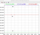
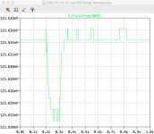
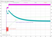
I also took the time to tidy up this part of my model. I had used the pre-supplied 2N5460 Vishay/Siliconix model for the JFET. It was delivering too much current (4x too much). I found Fairchild's MMBF5460 model and am now using that. Makes more sense now (predicted 8.84V) as do the modelled voltage drops across resistors R7-9. (Incidentally the model suggests there will be a modest variance between these of around 10mV. See attached chart. I have added also a closer look at R7's voltage drop for a 0->0.1A transient after 0.2s and back after 0.3s.)
At the moment, the model suggests minimal current (predicted 0.13uA) is being sunk by the 10V zener. I guess I could increase R10 to, say, 1K or more to rebalance the operation of Z1 and Z2?
Attachments
I am still bugged as to why a 2% voltage tolerance 10V zener (which had measured such previously) is reading closer to 9V...
... and the +/- xx% of your multimeter? ;-)
Relax, this is a total non-issue.
Re: capacitance: more cap does not necessarily help transient response. With 10 milliohms Zout, how much do you think this will be lowered with 2000uF // ?(hint: 2000uF at 20 Hz = 4 ohms...).
Personally, I have no prove that anything above a few 10's of uF is anything more than a waste of money and space.
What DOES make a difference is a good cap AT THE LOAD because ultimately, at those low impedances, several inches of wiring start to play a role, both ohmic and inductive.
Jan
Your circuit designer will need to create a list of possible alternatives, explore them, choose one, and verify it. Be sure to tell her any "management requirements" such as: must fit on existing PCB with no cuts or jumps, etc.I guess I could increase R10 to, say, 1K or more to rebalance the operation of Z1 and Z2?
It's an easy resistor change. But you guys are suggesting I am worrying about nothing. I was thinking that for the twin zeners to perform best that each should bear a decent share of the burden and the current being sunk was a decent indicator of this - from a lay point of view. (I will have a quick look at my model to see if this lay thinking is at all sensible.)
------------
I have removed the 1K resistor across the CE pads of Q3 and dropped in a new Q3. I removed two of the output caps (leaving 2 x 470uF) - stability analysis showed a significant difference in phase margin with two rather than one (whereas there was limited difference between two and four with respect to this). Jan's points are noted.
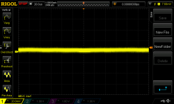
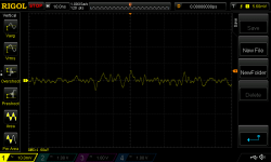
All seems well with voltage readings more or less in line with those in post #449. The issue seen previously and shown in post #378 is not there. (Is it my imagination that the base level of noise in that image is less than the current one attached below - I guess I could have had the intensity setting different or any other manner of variables could come into play including the different op amp. I presume it's meaningless until I get the rail connected to my measurement amplifier.)
Hopefully I am back to adding some load and rebuilding my chop chop box. I will also try to source parts for the gate-source protection circuit suggested by Mark.
Quite a saga getting to this point - I should not have made the board layout mistake re Z3 and certainly not placed C6 in the wrong way initially. With a bit of luck, when I have repaired the chop chop box it won't blow up again. 😱
------------
I have removed the 1K resistor across the CE pads of Q3 and dropped in a new Q3. I removed two of the output caps (leaving 2 x 470uF) - stability analysis showed a significant difference in phase margin with two rather than one (whereas there was limited difference between two and four with respect to this). Jan's points are noted.
All seems well with voltage readings more or less in line with those in post #449. The issue seen previously and shown in post #378 is not there. (Is it my imagination that the base level of noise in that image is less than the current one attached below - I guess I could have had the intensity setting different or any other manner of variables could come into play including the different op amp. I presume it's meaningless until I get the rail connected to my measurement amplifier.)
Hopefully I am back to adding some load and rebuilding my chop chop box. I will also try to source parts for the gate-source protection circuit suggested by Mark.
Quite a saga getting to this point - I should not have made the board layout mistake re Z3 and certainly not placed C6 in the wrong way initially. With a bit of luck, when I have repaired the chop chop box it won't blow up again. 😱
Attachments
Last edited:
I will have a quick look at my model to see if this lay thinking is at all sensible.
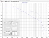
Increasing R10 improves Vref's rejection but there's little flow through to the broader circuit performance.
Attachments
Yet, when it all works, it can't hurt to check if the opamp can be supplied from Vout and it starts up.
But that's for later.
Jan
It's interesting to look at this. Supplying Vref from Vout doesn't do much at all, but powering the op amp from Vout makes a big difference to line rejection below about 600Hz. The way I have laid out the board provides an easy mechanism for Vref and the op amp to be supplied by Vout with a single wire connected between Vout and my 'jumper' R15 (with the removal of R6 and R8). But, yes, that's for later!
You know, I just realized that your MOSFET pass transistor does NOT contain any internal zener diodes to prevent VGS from exceeding the ±20 volt datasheet max. Nor does your board design.
Another way to go is to solder a pair of thru hole zener diodes in series (anode to anode) and tack solder this gizmo across the gate and source of a new MOSFET. Looking at the datasheet figure copied below, it seems you will get all the current you want (5A) with VGS < 5V so you could buy 4.7V zener diodes. Even if they have to drink the entire 50mA output current of the AD817 opamp that's less than half a watt.
I think this may well be a very real issue. I loaded the circuit with 1.5A and all was good. I then went to test with a 4.5A load and it appears the MOSFET has blown again. As a practical matter the circuit is never really going to start with a 4.5A DC load attached - the only load at startup is the output capacitance. (The true 'load' isn't connected until the voltages are up to spec as governed by my ATX PSU control board.) However, I currently don't have a mechanism for switching on/off the test load and it would seem the circuit protection is sensible in any case.
As I have taken my stock of the MOSFETS down from 6 to 4 already, I need to pick up a few more and Mouser is now out of stock. So I will have to head back to my original supplier in the UK, RS Online and I may as well grab other parts there. Their selection of zeners is limited. I presume any 0.5W circa 5V zener will be fine e.g. these.
In my opinion the easiest way to skin the cat is to work backwards from the power rating. Assume that during unhappy times (oscillation, startup, etc) the opamp is able to heroically source or sink 75 mA (50% more than its datasheet spec). So a 2W rated zener could be 27V, a 1W rated zener could be 13V, and a 1/2W zener could be 6.6 volts.
Notice that if you used a 2W or greater zener, you could simply connect a single zener to ground from the MOSFET gate node. If its zener voltage is more than 15V but less than 20V, it won't turn on during normal operation with Vout=12V, but it will prevent Vgate from exceeding Vzener.
Notice that if you used a 2W or greater zener, you could simply connect a single zener to ground from the MOSFET gate node. If its zener voltage is more than 15V but less than 20V, it won't turn on during normal operation with Vout=12V, but it will prevent Vgate from exceeding Vzener.
- 1N5931 3W 18V 21000 in stock at DigiKey USD 0.41
- 1N5355 5W 18V 15000 in stock at DigiKey USD 0.52
- 1N5354 5W 17V 3400 in stock at DigiKey USD 0.52
Last edited:
Two comments if I may: you really need only one zener across the G-S, with the K at the G. In the other direction the G is protected with the zener acting as a regular diode, sort of.
Second, at switch-on the output cap is discharged and acts as a short for the first few milliseconds. If you still have 2000uF there, that could well be the MOSFET slayer ;-)
Jan
Second, at switch-on the output cap is discharged and acts as a short for the first few milliseconds. If you still have 2000uF there, that could well be the MOSFET slayer ;-)
Jan
It's now 940uF 🙂
At max mains voltage the NTC in-rush limiter should be in place for about 430ms.
Another thought in relation to Jan's thinking - there's a lot of capacitance upstream of the pass device (much more than is behind it). It takes some time for this to charge to Vin and presumably quite a bit longer than it would take to charge the reg's output capacitance to Vout. So shouldn't Vds rise relatively slowly? The in-rush limiter also reduces Vin while the NTC is working. However if Vds is high the SOA of the MOSFET is a rather low current.
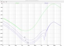
I have never been able to get to the bottom of why Vout in my 'AC-driven' model takes forever to rise - clearly a lot more than in reality. It takes about 10 seconds to reach 12V. It makes looking at these aspects via the model rather difficult. With the slow rise in Vout Vds does hit relatively high levels at peak UK mains - above 16V.
At max mains voltage the NTC in-rush limiter should be in place for about 430ms.
Another thought in relation to Jan's thinking - there's a lot of capacitance upstream of the pass device (much more than is behind it). It takes some time for this to charge to Vin and presumably quite a bit longer than it would take to charge the reg's output capacitance to Vout. So shouldn't Vds rise relatively slowly? The in-rush limiter also reduces Vin while the NTC is working. However if Vds is high the SOA of the MOSFET is a rather low current.
I have never been able to get to the bottom of why Vout in my 'AC-driven' model takes forever to rise - clearly a lot more than in reality. It takes about 10 seconds to reach 12V. It makes looking at these aspects via the model rather difficult. With the slow rise in Vout Vds does hit relatively high levels at peak UK mains - above 16V.
Attachments
Last edited:
If you had a Variac you could manually perform a very-slow-start. You could turn your wrist gradually and ramp the mains from 0VAC to 230VAC in 30 seconds. This would let you separately study (i) big DC load issues; (ii) big transient load {chop chop} issues; and (iii) startup issues.
Also as stated previously, a Variac would let you dial down the raw DC voltage to below 20V. High enough to produce regulated 12V but low enough to guarantee the VGSmax spec is met. Now if the MOSFET blows you know it's not a VGS issue, it's a SafeOperatingArea issue.
Also as stated previously, a Variac would let you dial down the raw DC voltage to below 20V. High enough to produce regulated 12V but low enough to guarantee the VGSmax spec is met. Now if the MOSFET blows you know it's not a VGS issue, it's a SafeOperatingArea issue.
One issue could be a slow rise of the ref. That will rise relatively slowly because the current source feeding it gets up to steam slowly because of C7 (I think) at 330uF which is charging slowly looks like. Make that 47uF and see if it goes faster.
Jan
Jan
If you had a Variac
They would appear to be very expensive unless I were to use a primitive mains light dimmer switch or similar
Last edited:
One issue could be a slow rise of the ref. That will rise relatively slowly because the current source feeding it gets up to steam slowly because of C7 (I think) at 330uF which is charging slowly looks like. Make that 47uF and see if it goes faster.
Jan
I think the bigger factor is the charging of the 470uF C8 cap filtering Vref.
But it doesn't seem to take 10 secs to get to 12V on the actual physical circuit.
They would appear to be very expensive unless I were to use a primitive mains light dimmer switch or similar
Us Yanks are pretty lucky I suppose; we have lots of hobbyist electronics stores and websites that sell good stuff cheaply. Here for example is a 2000 watt Variac for less than a hundred GBP but of course it is Yank input voltage and Yank frequency.
I wish I knew the names of comparable stores and sites in UK+Europe but alas, I don't.
UK Amazon offers this "Variable Transformer" but it's not a great price.
This is about as cheap as they get from mainstream suppliers CMV 2F-1 | Carroll & Meynell 1 Phase 480VA Variac, 1 Output, 240V ac, 2A | Carroll & Meynell
Maybe AndrewT has some ideas.
But I still think I'm grappling with a ghost. If it were the reg's output capacitance it would blow with no load attached and it didn't. I think the real issue - if due to SOA and I think it quite likely it is - a significant load (it was fine with 8R/1.5A but not with 8R in parallel with 4R / 4.5A) attached at switch on. Yet in reality there won't be a significant load at switch on as the load can't turn on until the output voltages are up to spec and then Vds is under 10V for peak mains, peak load.
I need a switch to be able to apply the load after turn on...
Nonetheless I will install the zeners across Vgs. I should get them tomorrow.
An element of progress. I fitted the two zener diodes across gate and source and installed a switch between the board and any external load. (If I do redo the board at some point I was thinking of using these SMD zener diodes.)
I can now comfortably switch in and out 4 Ohms in parallel with another 8 Ohms. (My multimeter reads a resistance closer to 3 Ohms for this test set up.)
I'm not inclined to remove the switch to see if the zeners were the cure alone. I now need to couple up the chop chop box again (but downstream of the switch).
Thanks for all the help getting to this point!
BTW I used a stop watch to measure how long it takes for Vout to come up to its stable level. The sim doesn't lie - it was much longer than I thought. I think I will halve the value of C8 when I can get hold of suitable parts.
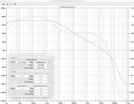
Lastly, it's worth noting the impact on phase response and unity gain frequency of shifting the powering of the op amp and Vref from Vin to Vout. See attached.
I can now comfortably switch in and out 4 Ohms in parallel with another 8 Ohms. (My multimeter reads a resistance closer to 3 Ohms for this test set up.)
I'm not inclined to remove the switch to see if the zeners were the cure alone. I now need to couple up the chop chop box again (but downstream of the switch).
Thanks for all the help getting to this point!
BTW I used a stop watch to measure how long it takes for Vout to come up to its stable level. The sim doesn't lie - it was much longer than I thought. I think I will halve the value of C8 when I can get hold of suitable parts.
Lastly, it's worth noting the impact on phase response and unity gain frequency of shifting the powering of the op amp and Vref from Vin to Vout. See attached.
Attachments
Last edited:
- Status
- Not open for further replies.
- Home
- Amplifiers
- Power Supplies
- Adventures with 5A regulated voltage circuits