I rearranged things as suggested by Brian, and moved a few other components to space things out a bit.
As for holes for ground connections on the board, I prefer not to. In the battle against ground loops (if one developes), I end up trying different things that are really better off not on the board.
Speaker grounds all ganged to the star ground, RCA inputs isolated (if needed) with low value resistor to split the ground. This resistor I would mount on the jack itself.
".................the filter need not be exact...."
That's quite true .
Would it help to use the second layer to duplicate power supply lines to reduce it's resistance ?
Cheers.
That's quite true .
Would it help to use the second layer to duplicate power supply lines to reduce it's resistance ?
Cheers.
ashok said:".................the filter need not be exact...."
That's quite true .
Would it help to use the second layer to duplicate power supply lines to reduce it's resistance ?
Cheers.
Darn! That's a good idea, but at this point it's too late...Gerbers already sent for pricing.
Ashok, where were you 2 days ago?🙂
Edit: I will increase trace thickness with soldered on wire.😉
ashok said:Would it help to use the second layer to duplicate power supply lines to reduce it's resistance ?
It probably wouldn't make any difference since the supply traces are already short and thick.
It might be a good idea not to take anything for granted while building circuits. Sometimes 'apparently' no problem tracks or routes could spring surprises , as I discovered many times.
However a VERY close inspection of the layout might show up 'flaws or possible improvements' . But Murphy and Friends are always around and will sometimes ensure that we miss the most obvious small errors or improvements!
One area where this is very widely experienced is in 'grounding schemes' ..............isn't it ?
So it always helps to use all choices available instead of implementing them later.
😀
ashok said:...Murphy and Friends are always around and will sometimes ensure that we miss the most obvious small errors or improvements!
One area where this is very widely experienced is in 'grounding schemes' ..............isn't it?
Yes, grounding is certainly critical to getting the most out of our circuits. Power and return paths should be given equal consideration and attention when routing a board.
Hi,
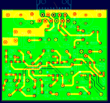
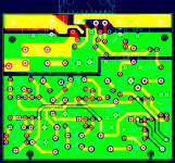
I'm not sure what I am seeing in that last PCB posting.
Are the decoupling grounds sharing a route with other returns?
I'm not sure what I am seeing in that last PCB posting.
Are the decoupling grounds sharing a route with other returns?
If that is one ground for all the returns then that is bad, very bad.
Are those thin yellow traces hard wiring or top side PCB traces.
The least you should do is star ground those returns.
Each decoupling pair should have a very short ground interlink and then to the power ground.
Each low current return deserves it's own trace, but some can share, on their way to a signal ground star.
Each high current or dirty current return demands it's own trace/wire and should ideally have a power ground star that can be sent to the central ground star whether on board or off board. Same philosophy as a power amp!
The thin yellow traces are actually red (the green topside copper pour makes them look yellow) and are on the bottom side of the PCB. The topside is the green ground pour.
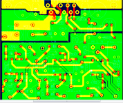
The high current ground paths for John's board should all be localized to the upper half of the board.
The high current ground paths for John's board should all be localized to the upper half of the board.
AndrewT said:If that is one ground for all the returns then that is bad, very bad.
Each decoupling pair should have a very short ground interlink and then to the power ground.
Each low current return deserves it's own trace, but some can share, on their way to a signal ground star.
Each high current or dirty current return demands it's own trace/wire and should ideally have a power ground star that can be sent to the central ground star whether on board or off board.
Andrew,
Ok, I need to get it straight. The grounding scheme in place now is no good? I can't see it.
My power supply for these has good filtering ( 14100 uF/rail ) with locale bypass caps. Also on the board are the 220 uF/rail plus bypass. The +/-15 v has 6800 uF/rail with locale bypass caps plus it's regulated. There can't be much left to clean up.
Also, as Brian said, the high current is at the top half of the board. Current will take the path of least resistance and exit via the main ground wire. Likewise, everything on the lower half is just shunt from the filter stages.
Nevertheless, I have delayed my board order and will go back to the drawing board for one final revision.
 Tomorrow night is the deadline though. As the power supply chassis is near complete, I need something to plug into it!🙂
 I will go with ashok's idea to bolster the +/- supplies on the board top, and I will split the ground plane, and add another ground connection as Andrew recommended.
I'm keeping an eye on this as I often wondered why no one had done what you are about to do!
I wish you success as you are doing what I said I'd do one day but never got around to it.
Keep up the good work!
I wish you success as you are doing what I said I'd do one day but never got around to it.
Keep up the good work!
Mikett said:
Keep up the good work!
Thanks Mikett. Feedback of any kind is great - positive feedback is the best!🙂
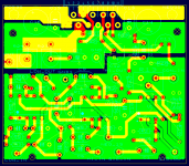
I have quickly make the changes. The new layout affects the top copper only.
As Brian mentioned, the yellow is the bottom copper layer(red) coming through the green top copper layer.
I have added a ground connection on the "signal" ground plane, which is not connected ( easier to physically connect the point with solder with the board in hand, than to edit the netlist, reassign pins). This will connect the lower part of the board via a seperate wire to a seperate star ground from all of the amp boards. I will then isolate this ground from the main ground with a 50 ohm resistor.
This should keep the two ground tribes from starting a ground war.

Attachments
Hi,
the decoupling caps are the dirty current sources. They are the very ones that can inject spikes and other nasties into the signal circuits.
I think from your description you now have this in hand.
Good luck.
the decoupling caps are the dirty current sources. They are the very ones that can inject spikes and other nasties into the signal circuits.
I think from your description you now have this in hand.
Good luck.
Thanks for you help Andrew. Your assistance is much appreciated🙂
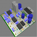
Have the final revision done and sent to Futurlec for manufacture. I have ordered 12 boards, enough for my current project plus a few more to play with.
Spent a little time cleaning the board up and added mounting holes.
Have the final revision done and sent to Futurlec for manufacture. I have ordered 12 boards, enough for my current project plus a few more to play with.
Spent a little time cleaning the board up and added mounting holes.
Attachments
A minor snag...Futurlec says my board clearances are too small (5 mil). Their minimum is 10 mil, so I've had to redo the layout yet again.
I removed pin 2 and 6 from the LM3886 to give a little more space. I also reduced the pad size on front row pins 1 to 11 to allow more clearance for traces between these pads.
I have re-emailed the files back. Hopefully, everything will be right this time.
I removed pin 2 and 6 from the LM3886 to give a little more space. I also reduced the pad size on front row pins 1 to 11 to allow more clearance for traces between these pads.
I have re-emailed the files back. Hopefully, everything will be right this time.
Attachments
Still no word from Futurlec. I have sent an email asking about the progress on the boards.
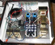
In the meantime, I have the power supplies complete. Fired it up last night and everything looks good. Correct voltages on all the outlets, no buzzing or humming. Dimmed the lights briefly since I don't have the soft start done yet.
One transformer, the one salvaged from the Akai amp, gets quite warm with no load. This is a 25-0-25 giving me +/-35 v. Anyone have any ideas?
Soft start: I have a nasty little MOSFET on order from Digikey (MTP3055) that I'm waiting on, plus 3-30 ohm 10 watt resistors and a 15 amp relay for this purpose. Using Rod Elliot's circuit (p39) for simplicity.
Yet another pic of the power supply chassis. The Akai transformer has a seperate 3volt winding that I have hijacked for the power LED. It will end up with one more tansformer - a 12 v for the soft start power on that I will add later.
Attachments
Andrew! That is the raddest idea! Ever! The whole alternative freq. and Q thing. ahh! man im so gonna be stuck on like 5 more projects! i love it.AndrewT said:Hi,
if you can arrange the components R3 & 4 and C2 & 3 to fit a DIL header and arrange the PCB with a DIL socket, you can swap out different headers with alternative frequencies and or Q values.
You can also swap C for R in each header by simply turning it around to convert from low pass to high pass (but this screws up the Q if you go for unity gain filter topology). If you go for equal value S&K then Q is set by the opamp gain and the Rs&Cs control just the frequency and not the Q.
This arrangement is very easy to change and saves a lot of PCB space by avoiding the need for the extra dual opamp and it's components.
Have you read the filter threads for the previous group buys? There is a lot more than just turn-over frequency and slope to consider when activating your drivers.
- Status
- Not open for further replies.
- Home
- Amplifiers
- Chip Amps
- Active filter plus LM3886 - one board