You are right, I simply missed the point, that the current on both sides are absolutely the same, so if there is 35mA on + , it is not possible to have 37mA on return. I would never use a mains supply with these distorsion figures. So we have to feed the board with a split battery supply, probably 12 (small) Lipofe cells, they make about 40 Volts, just an idea.Hey good thoughts, but I think the lack of a ground return in the middle (the virtual ground between the two shunt regulators) would still mess it up. So if that negative LM337 CCS were at 37mA, there would be nowhere for the extra 37mA - 35mA = 2mA to go at the input to the postive CCS. The board's draw would be the same, 25mA, and the extra 2mA could not go out through the 35mA CCS.
.
2.5 months in the mail for Victor's board
I just today received the 11kHz oscillator board that Victor mailed back on January 30th. 2.5 months in the mail! There has been a big port strike going on here for months that has slowed things down.
The board is just fantastic. 11kHz right on the money.
I just today received the 11kHz oscillator board that Victor mailed back on January 30th. 2.5 months in the mail! There has been a big port strike going on here for months that has slowed things down.
The board is just fantastic. 11kHz right on the money.
I would never use a mains supply with these distorsion figures. So we have to feed the board with a split battery supply, probably 12 (small) Lipofe cells, they make about 40 Volts, just an idea.
That would be an interesting way to do it! A dual rail battery supply. The board I did some preliminary work on a few posts back used all 9V primary (non rechargeable) cells. It would probably be possible to also allow that to be configured as a dual rail supply.
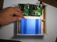
Power supply board finally going off to fabrication
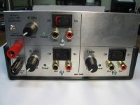
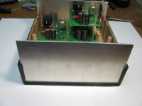
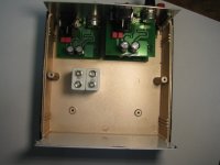
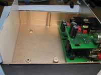
I wound up sidetracked on some other projects and haven't touched the power supply board for this project in six months! 😱 I've been using the case and front panel from the previous posts in this thread, with 3 of Victor's oscillators and a lab power supply: a 1Hz, 10KHz, and special order 11KHz.
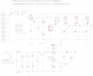
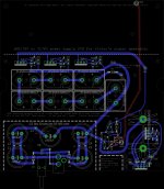
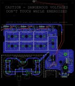
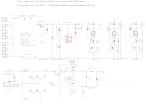
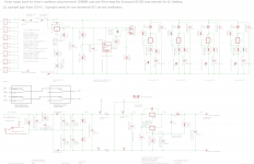
So time to fabricate that power board and get the case top on this thing! I've posted the schematic and layout below as png and pdf. The pdf can be zoomed in. If anyone should have any thoughts on ways to improve anything, please post! Much appreciated. Otherwise the board will probably go out to fab at the end of this week. If the board works when it gets back I'll post the Gerbers in case anybody else wants to use one. It is designed to fit in the case, but I also have 4 holes for 4mm standoffs so that it could also be used on a desktop or in some other larger case.
Details
I've designed the board to use either batteries or AC power, switch selectable. That small dotted line box near the back panel is where two panel mount switches go, that same type of rocker switch on the front panel. Recall the reason for that larger switch is to get a switch with a proper DC breaking rating. The small size switches max out at 28Vdc it seems.
There are three back panel switches. The one in the AC voltage doubler to cut AC power, then the two rockers panel mounted in back. One just cuts off the batteries while the other switches between AC or DC supplies.
The DC supply uses 7 PP3 "9V" sized batteries on end, mating with Keystone 968 PCB moutn end mount connectors. End mounting them makes best use of the vertical space in that tall Hammond case. I've specified 7 so it will work even with nearly dead batteries, and with either primary 9V cells (6.5Vdc min when dead, 9V max), rechargable 8.4V NiMH (7Vdc when dead, but no charger circuit built in here, 10.1Vdc fully charged), and rechargeable lithuium 8.4V cells (again no charger, they would have to be removed and charged offline, 8.4Vdc charged, 7.4Vdc "dead").
The top of the Hammond case comes off with 2 bolts and threads into metal studs. End mounting the batteries makes changing them easy.
The batteries then go via the AC/DC switch to pins feeding each Victor board through a 25mA constant current source. The CCS is made from a LM317HV regulator which is floating in this case. The 317HV is good for 60Vdc max input to output. One addition I've probably make it to add 56Vdc zeners from input to output on each. That not only protects the 317HV from capacitors grounding the output on startup t0+ with more than 60Vdc in, but in reverse performs that typical 317 reverse diode function from out to in to discharge output caps.
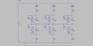
As for the CCSes, man that is a real head-scratcher! I actually gave myself a headache thinking about the interactions between the three Victor boards, with the center point of the TL431 current shunts all tied together via contact with the front panel. So LTSpice to the rescue. 🙂 The Spice plot below confirms that it works, but what happens is the tied-together center line adjusts as neeeded. I've purposely off-balanced the 3 "boards" in the sim by slightly changing the values of the 100R current shunt resistors. The effect is that instead of the midpoint being exactly 35Vdc/2 = 17.5Vdc it is more like 17.48 for one, then 17.452 for another, etc. Then when all three are tied together like this it finds a common value that is close to 17.5Vdc. The important thing is that this way the outputs of all three Victor boards really are ground-refenced to that same common ground tying the midpoints.
Just for fun I tried adding a second current source at the bottom, as rolls had suggested in one of the posts above. Sure enough, Spice won't even converge with the CCS fighting on top and bottom of each board. But if you leave just one CCS of the three off at the bottom (just the 100R resistor) it will converge. That one non-CCS point gives the whole thing enough adjust room to settle on a convergence point, if I have my head wrapped around this correctly. So long story short, just the one CCS per board.
I've also raised the system voltage enough so that the 100R resistors on Victor's board can be left as is. They don't have to be shorted across. Each 100R just drops 25mA * 100R = 2.5V, so I've bumped the system voltage up by 5Vdc. That is why the 7th. battery. The 317HVs are floating, not more than 60V in to out in any case, and the LR12 for the low battery LED is good to 100V.
Which reminds me, there is now the low battery LED circuit I was going to add. 🙂 The LR12 drops the voltage to 12Vdc to power a LT6703-3 comparator. Kind of a slick chip in that it has the internal reference & some hysteresis. The -3 is pre-wired the correct way for low battery. Saves parts and wiring. The chip is actually good to 36V. I may raise that output of the LR12, still thinking about it. The circuit just lights a LED, but I've extended the LED traces to the front panel between the Victor boards, to give a front panel indication.
The AC supply is a voltable doubler fed with 24Vac, which should generate somewhere around 68Vdc. That in turn is fed to yet another LM317HV (or TL783, either works but the 783 requires 10mA minimum load set resistors). That's a typo on the schematic, the output will be set for 45Vdc, so the 60V max in-out of the 317HV is not exceeded. I did put the protection zener on this one. I've designed it so the 317HV can be heatsinked either to the rear panel or to an on-board heatsink if the board is being used stand-alone. The regualtor just reduces ripple from the voltage doubler, of course.
But here is the slick part. That dotted line around the votlage doubler parts is the outline of 1/2 of a Box Enclosures B3-080 extruded aluminum case sawed in half on a band saw to become a B3-040 (the photo below is the whole B3-080 case). So although the board can be used as it sits, the metal case can be mounted there instead and all the AC votlage doubler parts put inside on card, to Faraday cage them. I'm just concerned that line harmonics EMI will get into the oscillators if this section isn't shielded like this, but maybe I'm over doing it. At any rate it should be a fairly ripple-free AC supply, being run through the vreg and then through the CCSes onto Victor's boards.
I wound up sidetracked on some other projects and haven't touched the power supply board for this project in six months! 😱 I've been using the case and front panel from the previous posts in this thread, with 3 of Victor's oscillators and a lab power supply: a 1Hz, 10KHz, and special order 11KHz.
So time to fabricate that power board and get the case top on this thing! I've posted the schematic and layout below as png and pdf. The pdf can be zoomed in. If anyone should have any thoughts on ways to improve anything, please post! Much appreciated. Otherwise the board will probably go out to fab at the end of this week. If the board works when it gets back I'll post the Gerbers in case anybody else wants to use one. It is designed to fit in the case, but I also have 4 holes for 4mm standoffs so that it could also be used on a desktop or in some other larger case.
Details
I've designed the board to use either batteries or AC power, switch selectable. That small dotted line box near the back panel is where two panel mount switches go, that same type of rocker switch on the front panel. Recall the reason for that larger switch is to get a switch with a proper DC breaking rating. The small size switches max out at 28Vdc it seems.
There are three back panel switches. The one in the AC voltage doubler to cut AC power, then the two rockers panel mounted in back. One just cuts off the batteries while the other switches between AC or DC supplies.
The DC supply uses 7 PP3 "9V" sized batteries on end, mating with Keystone 968 PCB moutn end mount connectors. End mounting them makes best use of the vertical space in that tall Hammond case. I've specified 7 so it will work even with nearly dead batteries, and with either primary 9V cells (6.5Vdc min when dead, 9V max), rechargable 8.4V NiMH (7Vdc when dead, but no charger circuit built in here, 10.1Vdc fully charged), and rechargeable lithuium 8.4V cells (again no charger, they would have to be removed and charged offline, 8.4Vdc charged, 7.4Vdc "dead").
The top of the Hammond case comes off with 2 bolts and threads into metal studs. End mounting the batteries makes changing them easy.
The batteries then go via the AC/DC switch to pins feeding each Victor board through a 25mA constant current source. The CCS is made from a LM317HV regulator which is floating in this case. The 317HV is good for 60Vdc max input to output. One addition I've probably make it to add 56Vdc zeners from input to output on each. That not only protects the 317HV from capacitors grounding the output on startup t0+ with more than 60Vdc in, but in reverse performs that typical 317 reverse diode function from out to in to discharge output caps.
As for the CCSes, man that is a real head-scratcher! I actually gave myself a headache thinking about the interactions between the three Victor boards, with the center point of the TL431 current shunts all tied together via contact with the front panel. So LTSpice to the rescue. 🙂 The Spice plot below confirms that it works, but what happens is the tied-together center line adjusts as neeeded. I've purposely off-balanced the 3 "boards" in the sim by slightly changing the values of the 100R current shunt resistors. The effect is that instead of the midpoint being exactly 35Vdc/2 = 17.5Vdc it is more like 17.48 for one, then 17.452 for another, etc. Then when all three are tied together like this it finds a common value that is close to 17.5Vdc. The important thing is that this way the outputs of all three Victor boards really are ground-refenced to that same common ground tying the midpoints.
Just for fun I tried adding a second current source at the bottom, as rolls had suggested in one of the posts above. Sure enough, Spice won't even converge with the CCS fighting on top and bottom of each board. But if you leave just one CCS of the three off at the bottom (just the 100R resistor) it will converge. That one non-CCS point gives the whole thing enough adjust room to settle on a convergence point, if I have my head wrapped around this correctly. So long story short, just the one CCS per board.
I've also raised the system voltage enough so that the 100R resistors on Victor's board can be left as is. They don't have to be shorted across. Each 100R just drops 25mA * 100R = 2.5V, so I've bumped the system voltage up by 5Vdc. That is why the 7th. battery. The 317HVs are floating, not more than 60V in to out in any case, and the LR12 for the low battery LED is good to 100V.
Which reminds me, there is now the low battery LED circuit I was going to add. 🙂 The LR12 drops the voltage to 12Vdc to power a LT6703-3 comparator. Kind of a slick chip in that it has the internal reference & some hysteresis. The -3 is pre-wired the correct way for low battery. Saves parts and wiring. The chip is actually good to 36V. I may raise that output of the LR12, still thinking about it. The circuit just lights a LED, but I've extended the LED traces to the front panel between the Victor boards, to give a front panel indication.
The AC supply is a voltable doubler fed with 24Vac, which should generate somewhere around 68Vdc. That in turn is fed to yet another LM317HV (or TL783, either works but the 783 requires 10mA minimum load set resistors). That's a typo on the schematic, the output will be set for 45Vdc, so the 60V max in-out of the 317HV is not exceeded. I did put the protection zener on this one. I've designed it so the 317HV can be heatsinked either to the rear panel or to an on-board heatsink if the board is being used stand-alone. The regualtor just reduces ripple from the voltage doubler, of course.
But here is the slick part. That dotted line around the votlage doubler parts is the outline of 1/2 of a Box Enclosures B3-080 extruded aluminum case sawed in half on a band saw to become a B3-040 (the photo below is the whole B3-080 case). So although the board can be used as it sits, the metal case can be mounted there instead and all the AC votlage doubler parts put inside on card, to Faraday cage them. I'm just concerned that line harmonics EMI will get into the oscillators if this section isn't shielded like this, but maybe I'm over doing it. At any rate it should be a fairly ripple-free AC supply, being run through the vreg and then through the CCSes onto Victor's boards.
Attachments
-
 IMG_3445.JPG136.7 KB · Views: 461
 -
 victor_pwr_supply.jpg139.6 KB · Views: 204
 -
pwr_supply_schematic.pdf26.7 KB · Views: 99
-
pwer_supply_layout.pdf64.6 KB · Views: 95
-
 pwr_supply_schematic.png53.7 KB · Views: 217
 -
 pwr_supply_layout.jpg568 KB · Views: 189
 -
 IMG_3449.JPG109.6 KB · Views: 364
 -
 IMG_3448.JPG126.8 KB · Views: 367
 -
 IMG_3447.JPG124.1 KB · Views: 458
 -
 IMG_3446.JPG141.1 KB · Views: 452
Last edited:
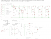
One revision already. 🙂 I've been debating whether to replace the LM317HV current sources with cascoded depletion mosfet sources. In the process of researching noise levels for the d-mosfet CCS luckily I've remembered Walt Jung's fantastic current source paper here
http://waltjung.org/PDFs/Sources_101_P2.pdf (opens PDF)
where he presents a depletion mosfet cascoding a LM317, with excellent low noise results as measured by his AP. As Walt mentions having the LM317 as the CCS device rather than a second d-mosfet results in more accurate and repeatable current values.
Plus this has the benefit of the power dissipation device (about 0.75W maximum) now being the DN2540 cascode mosfet. I've used the TO-220 version and once again spaced them where heat sinks could be added. Since there is just the d-mosfet Vgs of 3V or so across the LM317 now a TO-92 LM317L will do the job, 3V * 25mA = 75mW. Also luckily the 25mA number sits right in the middle between Walt's two plots, 16mA and 38mA.
I've converted the ground traces to polygons for lower Z. Click the lower lefthand corner of these png's to expand them.
Attachments
Last edited:
agdr,
Looking good. Wondering about your example here using the LM317 + depletion mode mosfet. for powering an opa134 18V+ and the LM337 + depletion mode mosfet for the 18V-.
I'm still looking to get your box for the oscillators too. : )
Looking good. Wondering about your example here using the LM317 + depletion mode mosfet. for powering an opa134 18V+ and the LM337 + depletion mode mosfet for the 18V-.
I'm still looking to get your box for the oscillators too. : )
SyncTronX - thanks! I've been pretty happy with how the front panels have turned out. 🙂
The LM337 is a bit of a problem since all the power depletion mosfets I'm aware of are n-channel. As an alternative to the LM317/LM337 pair consider using a LT3080/LT3015 LDO pair. I'm doing that right now with a project. Both are good for 30V input (the older LT1963A positive regulator is only good for 20V) and both can make use of a bypass capacitor on the reference set resistor to lower the noise. Plus both are LDO, needing only 0.5V or so across them vs. 3-5Vfor the older LMs.
Something interesting I noticed today in that old Walt Jung article I linked to above. Not only does he use an Audio Precision analyzer to measure the noise levels, in the acknowledgements section Bruce Hofer (AP) is listed as one of the article's reviewers.
Last edited:
I just today received the 11kHz oscillator board that Victor mailed back on January 30th. 2.5 months in the mail! There has been a big port strike going on here for months that has slowed things down.
The board is just fantastic. 11kHz right on the money.
The board does not appear to be currently available on eBay.
Are more in the pipeline?
The board does not appear to be currently available on eBay.
Are more in the pipeline?
Victor did a post a few weeks ago to PM him directly to buy boards:
http://www.diyaudio.com/forums/equi...on-audio-range-oscillator-83.html#post4380256
Sounds like the sales on eBay may have tapered off over time to the point where listing on eBay wasn't worth the cost anymore.
changes...
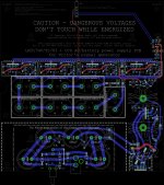
Lol, it is amazing how many small issues turn up when checking a PC board. 🙂 Lots of changes. This one will probably go out for fab on Monday.
* I discovered that I had the wrong width in for the B3-040 (B3-080 case cut in half) for the AC shielding inside the larger 1598EBK case. I was using 80mm when it should have been 107. So now the low battery circuitry is moved and the two rear panel switches are above the panel mount voltage regulator. Worked out well since there are also panel screw extrusions in the B3-080 case that would interfere with the top of the main filter capacitors if they are any closer than 7mm to the board edge. I have that marked on the PC board now. Also realized I hadn't taken the additional 2mm for the rear panel on the B3-040 case into account.
* Came to realized that a single ground polygon is a bad way to go with this particular topology. Each section is best off with twisted pair wiring going to the panel mount switches. Both send current and return in the same wire pair so the current flow in the twisted pair is equal and opposite. I have the two twisted pair wire holes in each section grouped together now. I've listed a wiring table at the top of the PC board. I've also included the panel switch wiring on the schematic, which shows how the twisted pairs from the board holes wire into the two rear panel switches.
* Related to the above, there is no longer a single "ground" listed on the schematic, since for the purposes here the circuit ground is that midpoint on Victor's boards between the two TL431 sections, a point that is off of the schematic (but connected to the front panel via the mounting of Victor's boards).
* Lots of obstructions to route around. 🙂 There are the four case bottom screw holes, which I now have text marking, the clearanes to the extrusions on the B3-040 case, and the area under Victor's board. I discovered I had that area sized wrong at 47mm rather than 52mm. Then there are those notches for the two case mounting posts.
* I've added a bilateral TVS suppression diode on the AC input.
* Haven't had the time to put a BOM together yet, but I do have the manufacturer part number (Mouser, Digikey, Farnell) marked now on the schematic for most parts.
* One kind of neat thing, I've added a dual-stack LED in front that can show through the front panel if the two holes are drilled. Fits right between the Victor boards. The top LED in the part is red and is the low battery warning indicator. The bottom LED is green and is just the power-on indicator when power hits the constant current sources feeding the Victor boards.
The pngs and PDFs below are the same, just a bit easier to zoom in on the PDFs.
Attachments
Last edited:
Victor did a post a few weeks ago to PM him directly to buy boards:
http://www.diyaudio.com/forums/equi...on-audio-range-oscillator-83.html#post4380256
Sounds like the sales on eBay may have tapered off over time to the point where listing on eBay wasn't worth the cost anymore.
Checking closed eBay listings shows a goodly number of completed auctions since then that were all completed as sales at the asking price.
2 in May, 4 in June and 2 in July.
No evidence of any listings that did not sell.
Checking closed eBay listings shows a goodly number of completed auctions since then that were all completed as sales at the asking price.
Hey that is good to know that Victor's boards are still actively selling!
Off to fabrication
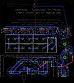
This thing is now out for fabrication. Lots of final changes, cleanup and adjustments. It passes DRC so it must work, right? 😛
* I remembered that I had created a front panel with 4 victor boards in the posts above. The Hammond case front panel can be drilled for 1, 2, 3 or 4 boards. I've added a 4th constant current source to the board and have drawn boxes around the 4 of them. If anyone else winds up using one of these just populate the number of current sources that match the number of Victor's boards you are using.
* The change above required moving the low battery circuit once again to free up space. The comparator parts are now behind the binding posts and the voltage regulator for the comparator is above the main heat sink. I had forgotten a bypass capacitor in the comparator section.
* The board can still be wired up to simply not use the per-board current sources at all (just don't populate them on the PC board), instead just set the main voltage regulator in the back for 35 volts and power the 1-4 Victor oscillators with that, as Victor had originally intended. Or that main voltage regulator can be wired as a single large current source (I have a placeholder for the resistor R16 that converts it, which is jumpered normally to use as a votlage source) that can be used to power board(s). Lots of flexibility in ways to use the board.
* As per the data sheets, and just good layout, I've added 0.22 uF film bypass caps on the inputs of either mounting location for the LM317HV regulators (heat sink or heat-sinked to the rear panel).
* I've addded a snubber to the AC voltage doubler section. I also realized the jumpers that act as disconnects if a B3-040 case is used in that area instead were in the wrong location. I've included a jumper that can be replaced with a picofuse if someone wants a fuse in it.
* The "safety" 56V zener across the LM317HV is now a 5W unit. Turns out the 5W is surge rated to some crazy thing like 3.2 amps, whereas there is no surge rating at all on the 1.3W diode. The reverse leakage is exactly the same for either zener and so is the price, so 5W it is.
* I had forgotten a datsheet-minimum output capacitor on the LM317HV's. Oops. Not strictly needed as with an LDO but apparently improves transient response.
* The AC voltage doubler section is now down to a single layer (PC board). I'm also about 90% of the way to transferring this circuitry to its own 100x40mm circuit board for use inside of the B3-040 metal case for sheilding. That will be a separate board to fabricate. I'm going to just populate the voltage doubler section on this one first and see how much line frequency noise, if any, gets into the oscillators without the metal shielding box around it.
* All the part values on the schematic should be correct now with manufacturer's part numbers by them.
Attachments
Last edited:
tubisy - I ordered just the minimum of 5 boards this time since there may very well be a screw-up. But assuming they do work I'm going to keep 2 of the boards and the other 3 will be up for grabs at-cost if anyone is interested. This run was $72.68 USD at Seeed Studio (China) including the shipping back to me. So that would be $72.68/5 = $14.54, plus actual shipping cost from the post office here, plus paypal's fee (2.9% plus 60 cents for US, 3.9% plus 30 cents for outside the US).
If there is a screw-up with this run then I'll be doing another one. 🙂
Once I get it tested and verified to work I'll also be posting the Gerber files so anyone can home-etch it or have their own board run done. The board is just 2 layers and nearly all the parts are through-hole, which I did on purpose to make for easy DIY soldering. The comparator in the low battery LED circuit is the only surface mount part since I couldn't find a through-hole comparator with a reference built in. All the good stuff appears to be SMD. But that entire low battery circuit can be left off, too.
In fact when I do the BOM I'm going to group it in sections so parts of the board can just be left unpopulated if someone doesn't need them. Like leaving off the battery snaps if it is only to be run on AC, or leaving off some of the 4 per-board current sources if less than two boards, or leaving off the entire AC voltage doubler and voltage regulator if the board is only to be run on batteries, or leaving off the low-battery indicator circuit. Lots of ways it can be wired.
As for fully assembled, if anyone is interested in that send me a PM. 🙂
I'm taking a completely opposite minimalist approach:
Board:
Ultra Low Distortion 0 00001 1kHz Sine Generator Assembled and Tested PCB | eBay
Chassis:
New Aluminum Project Box Enclosure Instrument Case Electronic DIY 100x76x35 mm W | eBay
Power supply (external):
48V 0 5A Poe Injector Power Over Ethernet Adapter for Wireless Access Point AP | eBay
Regulator chip:
5pcs TL783 TL783C High Voltage Regulators 125V to 220 A80C | eBay
From stock I'll add the remaining small parts, as well as a collection of output terminals including Dual Banana, XLR, TRS, and 3.5 mm
I wonder if there will be adverse measurable effects from the low road approach?
Last edited:
arnyk - thanks for that link to Victor's post, I see a problem in there! He has apparently cut the thickness of his latest board run to 1.2mm from 1.5mm. The ground screw hole will be 0.3mm further up. That will affect my panel CAD files. I'll add info about it in the first post in this thread.
Your plan there for boxing your board looks good, with the possible exception of that Ethernet power supply probably being a switcher. You might wind up with some switcher noise if the TL783 isn't able to filter it out. But, like you say, does it really matter. All that would likely do is put some spectrum lines up at 100KHz- 1MHz, wherever that switcher runs at, which might not be a big deal with the main signal at 1Khz or 10Khz.
That issue of switcher noise is why I went with a linear supply on the power board. Also why I added the snubber to eliminate that source of high(er) frequency noise.
If you are just putting one Victor board in the case you can probably adapt the single board front panel CAD file I posted for a Box Enclosures B3 case. The CAD program is a free download at Front Panel Express. Just remember to move the ground screw hole up by 0.3mm now!
Also remember the TL783 requires a higher minimum load current (than the LM317HV). I set my board up to use either (pinout and set resistor wiring is the same) but the 317 is more battery friendly if the set reistors are designed to be the minimum load. Figure 12 in the TL783 datasheet gives that minimum load vs. the voltage across it. You can probably get away with 7 or 8mA of minimum load. The datasheet table's 15mA is for the full 125Vdc across the part.
Last edited:
arnyk - thanks for that link to Victor's post, I see a problem in there! He has apparently cut the thickness of his latest board run to 1.2mm from 1.5mm. The ground screw hole will be 0.3mm further up. That will affect my panel CAD files. I'll add info about it in the first post in this thread.
Your plan there for boxing your board looks good, with the possible exception of that Ethernet power supply probably being a switcher.
I'd be very surprised it if is not a switcher.
You might wind up with some switcher noise if the TL783 isn't able to filter it out. But, like you say, does it really matter. All that would likely do is put some spectrum lines up at 100KHz- 1MHz, wherever that switcher runs at, which might not be a big deal with the main signal at 1Khz or 10Khz.
(1) Its like I have a big investment in the POE power supply. If it is too much of a pain, starting over costs me less than $10.
(2) The POE power supply could be put on a cord that is over 100' long, and I could put whatever EMI supression I want in line with it.
Also remember the TL783 requires a higher minimum load current (than the LM317HV). I set my board up to use either (pinout and set resistor wiring is the same) but the 317 is more battery friendly if the set reistors are designed to be the minimum load. Figure 12 in the TL783 datasheet gives that minimum load vs. the voltage across it. You can probably get away with 7 or 8mA of minimum load. The datasheet table's 15mA is for the full 125Vdc across the part.
The oscillator is speced to need 35 mA so unless Victor's spec sheet is a big fat lie, this should not be an issue, right?
Thanks for the comments, no matter what. Working alone is a bitch.
The oscillator is speced to need 35 mA so unless Victor's spec sheet is a big fat lie, this should not be an issue, right?.
That's right, if your Victor board is permanantly wired to the regulator that is all the load you need. In my case I have a switch between the regulator and board which would leave it with no load at times.
Hey please post your results when you get it all built! 🙂
BOM & build instructions
I've completed a first pass at the power supply board BOM and build instructions, attached below. I have the BOM sorted into sections of the board, such as batteries or AC voltage doubler or per-board CCS. Then the build instructions go into detail what each section does and the various ways they can be wired together.
I also have all the project materials out at a Google Drive linik now that I'll add to the first post in this thread:
https://drive.google.com/folderview...NUbmVvNFlhamVvSHlIMmZtbFJndHFiYk0&usp=sharing
The spreadsheet viewer on Google is really bad. I suggest using the download link for the BOM and viewing it in a spreadsheet program.
Attachments
Last edited:
- Status
- Not open for further replies.
- Home
- Design & Build
- Equipment & Tools
- A case and power supply for Victor's low THD oscillators