By the way, be sure any headphone amp you consider has both balanced and single-ended analog inputs 🙂
Will do!
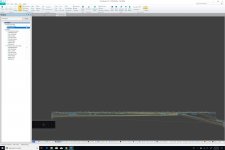
I don't think it's going to fit on a 2 × 1 board...
Here is what a 3 × 1 (110mm × 35mm) board looks like. This is probably a more realistic starting point...
Attachments
A friend of mine suggested two alternative preamps for the Audeze LCD-X:
Burson HA-160D
Shiit Jotunheim
I will listen to both of them next week in a shop that carries them in Tokyo.
I'm not sold on the value of this whole listening test, but I would not buy a product made by either Schiit or Burson. Maybe they have improved some, but a number of their products are not what I would consider well designed. I have not compared measurements but I bet the Massdrop THX amp is better than what you get from Schiit or Burson. If I were buying something, I would buy an RME ADI-2 Pro or Benchmark product.
This one is for the Altium Designer/CircuitStudio experts: the attached schematic generates the following PCB compilation error:
Nets Containing Multiple Similar Objects
It is described on this article.
I'm sure that I could get rid of the error by changing the pin type for the two IOUTL1N pins, but I'd like to avoid that. Any other way to work around the problem?
Or should I just edit the Connection Matrix? I don't really like this kind of hardcore solution either because it defeats the purpose of using proper pin types, but I can't think of anything else.
I tend to not use the pin/port types or set it to passive for problematic nets.
I'm not sold on the value of this whole listening test, but I would not buy a product made by either Schiit or Burson. Maybe they have improved some, but a number of their products are not what I would consider well designed. I have not compared measurements but I bet the Massdrop THX amp is better than what you get from Schiit or Burson. If I were buying something, I would buy an RME ADI-2 Pro or Benchmark product.
Thanks for the tip, much appreciated!
I tend to not use the pin/port types or set it to passive for problematic nets.
Got it! My perfectionism is getting in the way here...
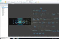
Monospace Font
Trying different monospace fonts for the overlay markings.
So far, Share Tech Mono is the best I could find.
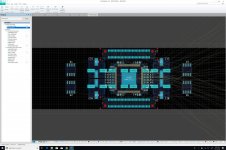
Also, trying to keep all the low small capacitors as close to the DAC chip as possible...
Trying different monospace fonts for the overlay markings.
So far, Share Tech Mono is the best I could find.
Also, trying to keep all the low small capacitors as close to the DAC chip as possible...
Attachments
I just became aware of this project (#8) and am just getting all the thread read.
But I haven't seen the question of multiple outputs vs mono addressed. I looked at the AKM sheet and was initially surprised to see the mono mode was voltage summing vs current summing before conversion as that is the methodology I am familiar with. I'm sure there are reasons to do that with this chip, that is for the manu to spec. But it does allow for an easy conversion on the back side to implement, especially in the way it is being conceived with the xlr board, where addition can occur. But, are there other concerns that need to be allowed for in the pin assignment and feeding?
Like I said, I still need to catch up on the reading, about half way there.
Cheers
Alan
WRT current summing versus voltage summing after I-V:
a/ The 4499 outputs so much current via such a low OP Z that if standard,
HQ audio opamps are used, there is not really much option but to voltage
sum.
b/ There is a separate feedback sense point for each channel. If you summed
all the current OP's then all the sense points would also have to be
connected and I'm not sure they would still work correctly.
c/ In 'mono' mode with all OP's current summed, both the super high current
swing combined with very low OP Z would render the need for a 'mini power
amp' type I-V. It seems a bit impractical.
d/ By using separate I-V opamps, the opamps noise is lowered by, in this
case, squ root of 8 = 2.83 x. This also works to achieve the -140dB DR spec.
T
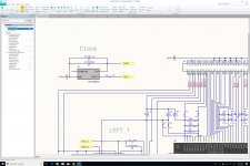
MCLK Circuit
I think I understand what the clock circuit should look like, but I am a bit confused about the output resistors. On page 55, we can see that we have a 51Ω (R1000) going from MCLK-DAC0 to MCLK, and on page 59 we have the famous 5.1Ω R1 going from the MCLK mezzanine pin to the MCLK DAC pin. Should both be mounted in series even if the clock is mounted much closer to the DAC chip than with the AKM reference board?
I think I understand what the clock circuit should look like, but I am a bit confused about the output resistors. On page 55, we can see that we have a 51Ω (R1000) going from MCLK-DAC0 to MCLK, and on page 59 we have the famous 5.1Ω R1 going from the MCLK mezzanine pin to the MCLK DAC pin. Should both be mounted in series even if the clock is mounted much closer to the DAC chip than with the AKM reference board?
Last edited:
Clock Circuit
Here is the schematic for the clock circuit.
Here is the schematic for the clock circuit.
Attachments
Last edited:
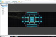
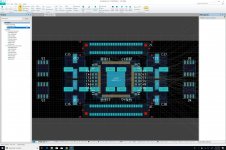
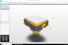
Non-Fool-Proof Connector Layout
This design for connectors is bad, because it does not prevent the incorrect mounting of the DAC board on the PSU board. Instead, we need to flip one of the connectors in order to get an asymmetrical layout. We will do that in the next revision.
This design for connectors is bad, because it does not prevent the incorrect mounting of the DAC board on the PSU board. Instead, we need to flip one of the connectors in order to get an asymmetrical layout. We will do that in the next revision.
Attachments
Last edited:
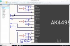
Just to make sure, I connected the circuits related to VCOM and EXTC to AVSS, not DVSS. The schematic is ambiguous about that, but I could not see how DVSS could be appropriate for this. Please correct me if I got this wrong.
To clarify, from AK4499 data sheet:
EXTCL1N O External Capacitor connection pin. This pin should be
connected to 1 µF to VSSL1.
VSSL1 us the analog ground for channel L1.
I think I understand what the clock circuit should look like, but I am a bit confused about the output resistors...
The series resistors are chosen to dampen any ringing on the high speed digital signals. The best value depends on the particulars of the implementation. The resistor values can be determined empirically by looking at the waveforms with a good, high-bandwidth scope and adjusting resistor values to maintain nice, square waveforms without ringing or with minimal ringing at the edge transitions.
...the AKM reference board, which uses the same crystal clock oscillator, uses a pair of 100pF and 0.1μF. We will go with the reference design.
The clock pads are unpopulated on the eval board. With a good ground plane and distributed bypass caps, a single decoupling cap is usually preferred. However, the square edges of a clock oscillator involve frequencies at odd harmonics of the fundamental. In the can of the dac clocks clock edges frequencies would go up to several hundred MHz and perhaps above 1 GHz. In that case, very low series inductance of decoupling caps is very important. The idea is to keep the resonant frequency of the capacitance and the series inductance very high, while keeping decoupling impedance low. The book you have, Ott, describes and explains the factors you should be considering.
Here is the schematic for the clock circuit.
If you are going to drive a remote USB board from local clocking on the dac board, you will almost certainly have to use a buffer chip to drive the lines. One line to the dac chip, and one to the USB board. Also you need two clocks, 49.152Mhz and 45.1584Mhz. The NDK SDA clocks have an enable pin to chose which one is in use. The signal telling you which clock should be enabled will come from the USB board. Each clock will need its own bypassing. There should be a dedicated 3.3v regulator for the clock modules. I would recommend to use ADM7150. The caps required for use with it are described in the applications section of the ADM7150 data sheet. For a clock buffer chip, would suggest NB3L553. Its data sheet describes what it needs in the way of bypass caps. Also, you will need a logic inverter chip to select one clock or the other based on a single signal from the USB board. The logic inverter will need power bypassing too. One example of some circuitry that shows much of what you might use can be found at: The ο1 precision master clock
Last edited:
- Home
- Source & Line
- Digital Line Level
- 8 × AK5578EN + 8 × AK4499EQ ADC/DAC Boards