I think I'll start with something "reasonable", like the LCD-X and a Massdrop THX 789. At $2,100, this combo is hard to beat. I'll train my ear on that, then upgrade to an HPA-1. Switching between the two pre-amps should help me appreciate the differences between switching power supplies and linear ones.
Do you have a decent 'normal system' ie; speakers + amp system to listen to?
HQ headphones are a fantastic 'magnifying glass' but I prefer speakers in a
room. Decent ones are expensive though.
Do you have a decent 'normal system' ie; speakers + amp system to listen to?
HQ headphones are a fantastic 'magnifying glass' but I prefer speakers in a
room. Decent ones are expensive though.
My workshop is in a garage, so loudspeakers would not sound great.
Better work on constructing a setup to enable blind, level-matched tests 😉.
How would you go about doing that?
Better work on constructing a setup to enable blind, level-matched tests 😉.
How would you like to measure the level matching?
How would you go about doing that?
You don't remember that either? It's okay, I didn't think it likely. Just ribbing you a bit.
I have some material you can download to practice with.
How would you go about doing that?
I'm not really suggesting you have to (I wouldn't waste my time, personally). I just posted that as a response to the unsubstantiated opinions overrunning the thread now, under the guise of critical research.
Sighted listening tests are worse than worthless, in my opinion.
How would you like to measure the level matching?
Probably good enough with a low frequency sine test tone and a calibrated true RMS DVM.
Last edited:
North-West Side
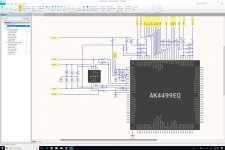
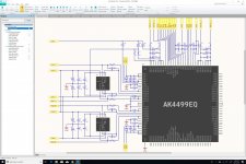
Here is the North-West side of the schematic. I am using ports for the time being, but most of them will be replaced by proper connectors once the full schematic is laid out. Unless I missed something, the rest is nothing more than a repeat of what we have right now, with the South side being a bit simpler than the North side. I hope to have it completed by tomorrow. I'm sure that it can be improved quite a bit, but it's already a lot more readable than AKM's. I just hope that I positioned the polarized capacitors the right way... Please let me know if you can spot any mistakes (assuming that you have access to the evaluation board's manual). After that, I'll probably need some help laying out the circuit for the clock, but we can discuss that once the baseline schematic is complete.
Here is the North-West side of the schematic. I am using ports for the time being, but most of them will be replaced by proper connectors once the full schematic is laid out. Unless I missed something, the rest is nothing more than a repeat of what we have right now, with the South side being a bit simpler than the North side. I hope to have it completed by tomorrow. I'm sure that it can be improved quite a bit, but it's already a lot more readable than AKM's. I just hope that I positioned the polarized capacitors the right way... Please let me know if you can spot any mistakes (assuming that you have access to the evaluation board's manual). After that, I'll probably need some help laying out the circuit for the clock, but we can discuss that once the baseline schematic is complete.
Attachments
Last edited:
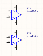
Haven't had a chance to look closely but noticed an aesthetic thing. I would definitely redraw your op-amp symbol as an op-amp, not a box. Makes it much easier to read.
Haven't had a chance to look closely but noticed an aesthetic thing. I would definitely redraw your op-amp symbol as an op-amp, not a box. Makes it much easier to read.
I can certainly do that. Will post an updated version tomorrow.
Thank you Chris.
Haven't had a chance to look closely but noticed an aesthetic thing. I would definitely redraw your op-amp symbol as an op-amp, not a box. Makes it much easier to read.
Here is the best that I could come up with. Please let me know if you had something else in mind.
Attachments
That's better, although normally I see them like this. Multipart A/B for duals.
Unless it's only a few pins, normally I don't even use 4-sided schematic symbols. I just use two and break it up into parts. I usually group the pins according to function as well. This is all optional, but I find it makes the resulting schematic easier to read.
Unless it's only a few pins, normally I don't even use 4-sided schematic symbols. I just use two and break it up into parts. I usually group the pins according to function as well. This is all optional, but I find it makes the resulting schematic easier to read.
Attachments
Last edited:
That's better, although normally I see them like this. Multipart A/B for duals.
Unless it's only a few pins, normally I don't even use 4-sided schematic symbols. I just use two and break it up into parts. I usually group the pins according to function as well. This is all optional, but I find it makes the resulting schematic easier to read.
I think I get your point. I like to do that as well, but in this particular instance the chip is so very symmetrical across two axes that preserving the physical layout is quite conducive to a clean schematic, and provides a good first step toward the PCB. I also wanted something that is not too far away from the original schematic, so that we have a clear point of reference.
That being said, the schematic that I am currently working on might turn out to be nothing more than an intermediary step toward a more abstract schematic that is much closer to what you had in mind. We'll see...
The output stage application examples in the AK4499 data sheet show the opamps in conventional form and layout, aside from the power terminals. Sometimes those are shown separately anyway.
Last edited:
Part Designator Scheme
Here is a first crack at the new part designator scheme.
The idea is that the circuit is made of four symmetrical sections:
1. Left 1
2. Right 1
3. Left 2
4. Right 2
With that in mind, a Left 1 capacitor will be designated CX1 or CX5, with X being any number from 0 (then omitted) to 9. The corresponding capacitor on Right 1 will be designated CX2 or CX6. And the same goes for Left 2 (CX3 or CX7) and Right 2 (CX4 or CX8). That way, it should be relatively easy to locate any component on the schematic, or to designate any component for which the corresponding component on another section is already designated. CX0 and CX9 are kept for components that do not belong to these symmetrical sections. And the same goes for resistors or diodes.
This spreadsheet provides a convenient lookup table to go from one to the other.
Attachments
Last edited:
The application example in the AK4499 data sheet show the opamps in conventional form and layout, aside from the power terminals, that is. Sometimes those are shown separately anyway.
That's right. The schematic on the datasheet looks like a schematic, while it looks like a PCB on the evaluation board's manual. I am trying to find a happy middle ground with our schematic.
Big black blobs are not so great if one wants a printout. There goes the black ink cartridge...
Big black blobs are not so great if one wants a printout. There goes the black ink cartridge...
That's true. I noticed the same thing this afternoon. They look good on screen, but they're stupid on paper. I'll make sure to provide both versions when I'm done.
West Side
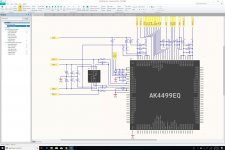
Here is the West side (L1 & R1) fully laid out.
Note how the two operational amplifiers are aligned with each other, instead of being rotated from each other. This means that the indices of designators are in correspondance with respect to the operational amplifiers, but not with respect to the DAC chip. It's one or the other, it can't be both, so we picked one (the former), because it creates clean I-V blocks.
Also, we're now using red pads to terminate non-connected pins (like the four NC pins found on the DAC chip). This looks much cleaner than leaving some floating pins. I just hope that it won't create any problem when we lay the PCB out.
The hardest parts of the schematic are probably behind us now.
Now working on the East side (L2 & R2).
PS: As much as I do not like AKM's schematic for this board, I love their pinout for the AK4499EQ chip. It's designed in a really logical way that makes the schematic super clean, and it should really help with PCB layout, as can be seen on the evaluation board (very simple and symmetrical traces).
Attachments
Last edited:
- Home
- Source & Line
- Digital Line Level
- 8 × AK5578EN + 8 × AK4499EQ ADC/DAC Boards