IIRC Scott Wucer said it was sent to him in a confidential document from ESS when Scott was trying to help them find some problems with their dacs. He is a an old friend of Martin Mallinson, ESS engineering VP. Scott said he thought it would be okay with ESS if he just shared that one pic, which he posted in another thread (IIRC it was in one of PMA's listening test threads). The pic shows a time domain view of a low level 50Hz test signal after processing by a notch filter, then amplified by an LNA. In other words, it is a distortion residual....TBH I highly doubt that this is a real measurement...
Also IIRC, I believe Scott's point in posting it was to show that typical FFT measurements provided at the push of a button by a fancy AP machine is not all there is; it is over-relied upon by many people. He also commented about the over-reliance issue in the Black Hole thread.
Last edited:
Agreed. The diyinhk board used something more or less like ESS datasheet I/V conversion and differential summing. Nonetheless, the boards themselves are poorly designed and IME they sound like it....it is not the IV stage used for the DIYINHK ES9016 DAC...
@InspectorGadget: The time I spent with cheap ESS dac boards was to find out if there was an easy way to make them sound better for low cost hobbyist projects. After a lot of effort it turned out there was not an easy way, although there is a hard way. Not worth the trouble, would be my conclusion at this point.
for anyone trying to go of this schematic: it is not the IV stage used for the DIYINHK ES9016 DAC. Can't find my notes, but certainly no AVCC connection, no coupling cap and resistors on the output. Just 780 ohm and a parallel cap in the feedback loop (inv), resp to ground (non inv).
Youre right, cant see any output caps. So still not really going to be truly an IV stage if its driving the non inverting input with the +out, is it?. I cant think of a way to do a 8 ch BAL->SE summed IV stage for ESS with only 4 x dual opamps. So, looking closer at the 'IV' stage. and with your description to match, it looks like the inverting side is an IV stage, but the non-inverting is not. non-inverting inputs are typically high impedance, the ESS requires to be driving a virtual ground (non-inverting, preferably biased to some fraction of AVCC. the exact voltage will depend on the dac, they are all different) so all in all a bit odd. its late here, so maybe my thinking is scrambled.and the only pics available are pretty low res.
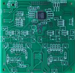
Attached below are pics of the diyinhk board I received. One can compare them to the ESS ES9038PRO eval board gerbers in the board documentation package available for download at: https://ismosys.com/wp-content/uploads/2020/08/ES9038PRO-8CH-Ver-1.3.zip
Attachments

Last edited:
Oh I know Mark.Agreed. The diyinhk board used something more or less like ESS datasheet I/V conversion and differential summing. Nonetheless, the boards themselves are poorly designed and IME they sound like it.
@InspectorGadget: The time I spent with cheap ESS dac boards was to find out if there was an easy way to make them sound better for low cost hobbyist projects. After a lot of effort it turned out there was not an easy way, although there is a hard way. Not worth the trouble, would be my conclusion at this point.
ha!! yeah thats one of the old ones. what a mess.
Ah, perhaps it was the test Scott used that was designed by Samuel Groner, rather than being performed by him. it was definitely mentioned over on the hump investigation thread on ASR.
https://www.audiosciencereview.com/...ess-thd-‘hump’-investigation.5752/post-743823
Without defining what sound better is in specific context, such description is meaningless.to find out if there was an easy way to make them sound better
should have said ... the ESS requires to be driving a virtual ground (or very low impedance), for current out. Just in case people didnt catch the inference. Sorry, the edit window closed. and with that I bid you guys goodnight.
the 8-channel board has a totally different layoutAttached below are pics of the diyinhk board I received. One can compare them to the ESS ES9038PRO eval board gerbers in the board documentation package available for download at: https://ismosys.com/wp-content/uploads/2020/08/ES9038PRO-8CH-Ver-1.3.zip
As I understand from this image, instead AVCC connection to opamp ininverted input, it has resistor and parallel capacitor to ground, resistors are probably 780 ohm.for anyone trying to go of this schematic: it is not the IV stage used for the DIYINHK ES9016 DAC. Can't find my notes, but certainly no AVCC connection, no coupling cap and resistors on the output. Just 780 ohm and a parallel cap in the feedback loop (inv), resp to ground (non inv).
Yeah, thats how I understood it. So yes, the dac driving the inverted input is running in current mode, but the dac driving the non-inverting input is driving a higher impedance node, because non-inverting inputs are much higher input impedance, as well as this phase just seeing a resistor and cap to ground. the negative feedback means the inverting input node resembles a virtual ground ie very low impedance, thats the point. so this is a very odd 'IV stage' indeed. not even sure what the DAC chip would make of having such different loads on each pin. I would think the whole thing would just run as a voltage buffer, with the dac outputting voltage, but i'm not sure. Here i've just done up a scheme of what it looks like. Following is a snip of the first stage in the es9038PRO app note. obviously the AVCC isnt relevant, as they didnt add that, but you can see both phases feed the inverting node and then there is a following summing stage for the SE outputs, or just take the balanced outs directly after this (well, after the output filter)
Someone should make a decent multichannel IV to connect to the outputs of this. I prefer all on one board, but you would get better performance than using the onboard. that would only be worth it if you already owned the board IMO. better ways to spend the money otherwise.


Someone should make a decent multichannel IV to connect to the outputs of this. I prefer all on one board, but you would get better performance than using the onboard. that would only be worth it if you already owned the board IMO. better ways to spend the money otherwise.
Last edited:
Well aware of these posts, I have made comments there and had a personal conversation with the author, Michael, after he posted. So no hypocrisy here, I did my work. The post you referenced is about the ES9016, though, not the ES9038. No measurements from this board anywhere, just some preliminary data and him saying he is so satisfied with the ES9016 that there is no reason to go to the ES9038. Michael told me he did some more -unpublished- measurements on the ES9038, and it was - with some more care - easily measuring better SN than the ES9016. But this is besides the point: the ES9038 implementation was criticized without proper data.
I don't understand your criticism about the modular approach DIYINHK uses; it's ideal for the DIY-er we are supposed to be here. Proper implementation (short low impedance wiring, etc) is what DIY is all about IMHO.
But I should not have singled you out, for that I apologize. My disappointment on the quality of the posts and the level of prejudice and non-informed opinions got to me. Especially when my precious dac under attack. 🙂
I had been lurking in the background on this thread but missed this post.
Just to clarify I did NOT say the ES9038 had better measuring SN than the ES9016. I said that the noise performance was as good as the ES9016 (of course this is limited by the MOTU M4 ADC noise) but the distortion performance was worse and well within the bounds of what the MOTU M4 can measure. In addition as discussed previously there is significant variation between the channels.
For reference here are some quick measurements of the ES9038 with the MOTU M4 with one channel driven. These measurements use the standard I/V stage and a linear power supply. Power supply wiring is directly soldered to the DAC board. Output level is full output (2 V).
Channel 1 (outer board position).
Channel 3 (inner board position).
I really do not see any reason to go with these DIYINHK DACs. By the time you add power supplies, case and I/V stages you are probably approaching the cost of a well engineered multichannel DAC like the MOTU Ultralite Mk5 and even then you have no guarantee on how it will perform.
Michael
From datasheets can be find ES9016 analog output impedance is 834 ohms, ES9038pro is 202. Maybe this is cause why with this IV stage give with ES9016 board better results, DAC chip + and - output current difference is smaller with ES9016 chip.Yeah, thats how I understood it. So yes, the dac driving the inverted input is running in current mode, but the dac driving the non-inverting input is driving a higher impedance node, because non-inverting inputs are much higher input impedance, as well as this phase just seeing a resistor and cap to ground. the negative feedback means the inverting input node resembles a virtual ground ie very low impedance, thats the point. so this is a very odd 'IV stage' indeed. not even sure what the DAC chip would make of having such different loads on each pin.
In this IV stage noninverted input is not grounded and inverted input will had no ground potential but even less (in opposit phase with inverted signal), in way that current from ES chip inverted output will be bigger than with grounded noinverted opamp input.
Thanks for the clarification! I guess I interpreted 'Noise performance was at least as good as the 9016 (limited by the MOTU M4 ADC noise)' too optimistically. I agree that the stock IV stage on the board is no more than a means to get you going. I am using it with 4 Twisted Pear IVY III stages instead. The ES9016 had audible noise from the speakers, the ES9038 is dead silent now. Maybe not the cheapest way, but I like tinker incrementally this way, and it sounds great in the end. And that's what it's all about. Btw I am now using Cantabile as a vst host for XO and DSP; very nice to work with and to my surprise it sounds better than vst in Foobar2000I had been lurking in the background on this thread but missed this post.
Just to clarify I did NOT say the ES9038 had better measuring SN than the ES9016. I said that the noise performance was as good as the ES9016 (of course this is limited by the MOTU M4 ADC noise) but the distortion performance was worse and well within the bounds of what the MOTU M4 can measure. In addition as discussed previously there is significant variation between the channels.
For reference here are some quick measurements of the ES9038 with the MOTU M4 with one channel driven. These measurements use the standard I/V stage and a linear power supply. Power supply wiring is directly soldered to the DAC board. Output level is full output (2 V).
Channel 1 (outer board position).
View attachment 1011565
Channel 3 (inner board position).
View attachment 1011566
I really do not see any reason to go with these DIYINHK DACs. By the time you add power supplies, case and I/V stages you are probably approaching the cost of a well engineered multichannel DAC like the MOTU Ultralite Mk5 and even then you have no guarantee on how it will perform.
Michael
@kaameelis
No.
they are completely different distortion mechanisms in 9016 and 9038. 9038 board outputs much higher current than 9016 ( havent checked to see what they do with AVCC bias if anything in the 9038 board. dont know if its exactly the same as this or not).
9016 was more accepting of higher AVCC bias (none on the board though) indirectly yes, but not for the reasons you state. the 9038 wants about AVCC/3 bias on inverting inputs to avoid the IMD hump being visible above the noise, but the output still swings around AVCC/2 (close) the remaining current is then supplied from the IV stage opamp negative rail. 9016 is the same, but it wants closer to AVCC/2, for different reasons.
When running in 'current mode' and 'voltage mode' its not so much that the DAC puts out more current, its that more of the same current is converted to voltage in the DAC, depending on how high the resistance to ground it sees is at its output. As a trans-impedance stage neg feedback node acts as a virtual ground, or maybe better explained as a virtual short to it (it has nothing to do with being connected to ground), this resistance is made effectively very small compared to the dac output impedance, so current flows and the opamp measures the voltage difference between its inverting input (virtual ground) and its output across the resistor. on the non-inverting rail; the dac sees a resistor to ground in parallel to a very high impedance, thus effectively just sees the resistor to ground and this voltage is what the opamp sees and compares/adds voltage across its negative feedback loop. so its the distortion that will be different on each phase and therefor not cancel much, including the distortion and noise from the AVCC regulator; as the loading on each side is different. That is but one (the main) mechanism, I suspect.
the 9038 board outputs about +/-15ma, so depending on the opamp used, this, along with having to source some of the dac current too, mean that some will be operating outside their capability. with the 9016, the current is much smaller (about 4 times), so the opamps will handle it comfortably. I cant remember how profound the difference in performance was with driving a virtual GND at 0V vs biased, but it was significant. its unknown quantity makes it difficult to describe the whole theoretically.
both halves of the DAC are swinging around the same AVCC/2 mid point (this is simplified, the equation is a touch more complicated than that) there will at least not be a DC offset. both + and - dac output swing around a middle point between AVCC and GND, usually 1.65VDC. this has no effect on the voltage at the inverting input node of the opamp, its negative feedback is constantly adjusting to the center voltage of its own rails, unless you bias it with positive feedback of a fraction of AVCC. So for best results, it is better if the DAC sees a virtual ground biased to the same potential as its own internal virtual ground. ~1.65VDC, vs 0vdc virtual ground we see on the 9016 dac (I havent worked with this part specifically, just 9018/9012/9028/9038q2m they all want slightly different bias for best performance)
Right. I think i've said enough on this subject and the more I keep rehashing the same content off the top of my head and trying to expand on it for people, the more chance there is of me making a mistake. as far as I know, aside from some omission of some mechanisms etc, i've already said all that needs to be and havent made any glaring errors. please read up on the subject matter before trying to correct me. I dont want to have to take on a research project just so I make sure that everything I say in a detailed rundown is correct, so that someone who should have looked themselves, understands. Sorry I dont mean to be blunt, but ive had about enough of this thread. Everything I predicted or repeated is correct (aside from the early agreeing with you about what the IV stage looked like without double checking a detailed photo ie, output caps and AVCC connection etc) and has also been confirmed by experiment thanks to Michael. There is obviously some other layout issue effecting the different channels on the 9038 IV that I havent talked about, investigating that without the actual board to measure and dissect is a pointless endeavour.
I'm not here to redesign someone elses dac, when i'm lacking time and energy to work on my own. they effectively took the cheapest, worst performing option in the old app notes that ESS doesnt even fully specify or recommend and removed even more parts from it; so its not like they will ever do anything up to standard IMO.
please read these 2. it will see these 2 circuit types on each input.
https://ultimateelectronicsbook.com/op-amp-transimpedance-amplifier/
https://ultimateelectronicsbook.com/op-amp-voltage-buffer/
Last edited:
Thanks for the clarification! I guess I interpreted 'Noise performance was at least as good as the 9016 (limited by the MOTU M4 ADC noise)' too optimistically. I agree that the stock IV stage on the board is no more than a means to get you going. I am using it with 4 Twisted Pear IVY III stages instead. The ES9016 had audible noise from the speakers, the ES9038 is dead silent now. Maybe not the cheapest way, but I like tinker incrementally this way, and it sounds great in the end. And that's what it's all about. Btw I am now using Cantabile as a vst host for XO and DSP; very nice to work with and to my surprise it sounds better than vst in Foobar2000
I just realized that I have an Ian Canada I/V Std MkII lying around and like you I like to tinker so I am considering seeing what it can do.
These questions will display my ignorance but when using an external I/V do I still need to connect the AVCC power supply to the DAC board? Obviously the I/V needs an AVCC connection but unsure if the DAC board still needs it. Similarly I assume that the +/- 12 V connection to the DAC board is not needed and I only need to connect it to the I/V, is this correct?
Thanks,
Michael
No problem Michael. The community owes you a debt of gratitude for taking one (two?) for the team, pushing ahead to make your own mind up, in spite of opinions like mine around the place on these boards (I totally understand and respect why you did mate) not only that, you took on the task of measuring your progress, so people can actually see what ive been harping on about, without me having to buy them 🙂. Also, thanks for the backup to confirm your position.
So. to your questions
where is ians schematic? does it have a proper connection for AVCC bias? this take the form of a voltage input, usually a fraction of AVCC, ether via a voltage divider from the DAC AVCC regulators, or you can also supply your own dedicated bias to feed into the non-inverting input of the opamps. without looking at ians schematic, I cant give more specific advice. his opamp IVs are pretty simple too, he favours transformer 'IV' conversion, so low harmonic distortion is obviously not that important to him 🙂. hes certainly very competent, but this isnt really his area of main interest; he tends to leave the analogue to others, for the most part. this voltage input is connected to a series resistor and then the cap to ground to buffer that voltage. see the second pic I linked above, the snippet of the balanced opa stage from e9038pro app note. but thats not the whole circuit, there is more (the voltage divider) connecting to the AVCC regulator.
yeah, I would tyhink its safe to leave it unconnected to the dac board. I dont think there are any other regulators feeding off the 12V supplies, just the opamps.
hope that helps. feel free to PM me if you have any other questions.
So. to your questions
Yes. depending on the AVCC bias amount present on ians boards, most current for the dac output will be supplied from DAC AVCC, but as that bias amount goes down with respect to AVCC/2 (or whatever the particular dac is expecting) more of that current for the output is sourced from the opamp negative power rail. you still always need the AVCC supply on the dac board though, it powers the analogue section, without it, the dac will output nothing. The dac uses this voltage as a voltage reference that the modulator is compared to. ie the dac modulator, modulates this voltage directly.do I still need to connect the AVCC power supply to the DAC board?
Obviously the I/V needs an AVCC connection but unsure if the DAC board still needs it
where is ians schematic? does it have a proper connection for AVCC bias? this take the form of a voltage input, usually a fraction of AVCC, ether via a voltage divider from the DAC AVCC regulators, or you can also supply your own dedicated bias to feed into the non-inverting input of the opamps. without looking at ians schematic, I cant give more specific advice. his opamp IVs are pretty simple too, he favours transformer 'IV' conversion, so low harmonic distortion is obviously not that important to him 🙂. hes certainly very competent, but this isnt really his area of main interest; he tends to leave the analogue to others, for the most part. this voltage input is connected to a series resistor and then the cap to ground to buffer that voltage. see the second pic I linked above, the snippet of the balanced opa stage from e9038pro app note. but thats not the whole circuit, there is more (the voltage divider) connecting to the AVCC regulator.
Similarly I assume that the +/- 12 V connection to the DAC board is not needed and I only need to connect it to the I/V, is this correct?
yeah, I would tyhink its safe to leave it unconnected to the dac board. I dont think there are any other regulators feeding off the 12V supplies, just the opamps.
hope that helps. feel free to PM me if you have any other questions.
Last edited:
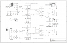
Iancanada output stage schematic attached.
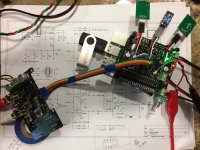
Links not workinig, so some more pics below about dealing with noise problems when connecting Ian's dac stack. Basically there was noise coupling between the boards that was easily audible. Even with a ribbon cable to add some distance between the dac board and the output stage board, I found that folding over and taping the ribbon cable in a certain way canceled out some more noise. The other pics shows the dac board being separated from the FIFO_Pi by a right angle adapter. Some of these discoveries preceded Ian's development of some shielding solutions that are available now.
EDIT: Rotated schematic for easier readability.
Attachments

Last edited:
cool, so the connection is there at least, with enough opamp channels to manage it properly.
just glanced, so sorry no feedback and havent read any links. its bedtime for me, so I probably wont, either. 😛
Mark will sort you out, but as I said, feel free to PM me. i'll have a squizz tomorrow night
just glanced, so sorry no feedback and havent read any links. its bedtime for me, so I probably wont, either. 😛
Mark will sort you out, but as I said, feel free to PM me. i'll have a squizz tomorrow night
Last edited:
Thanks for the info guys, I have a slightly newer version of the I/V, the schematic for which can be found here -> https://github.com/iancanada/Docume...acHAT/IVboards/IVSTD/IvStdMkII_ManualV2.0.pdf.
I assume Vref is the AVCC bias and based on the voltage divider looks like it is set to AVCC / 3.
So in terms of supplying AVCC to Ian's board and the DAC I assume that I just split it at the regulator output?
I'll give it a try this weekend and see how it goes.
Michael
I assume Vref is the AVCC bias and based on the voltage divider looks like it is set to AVCC / 3.
So in terms of supplying AVCC to Ian's board and the DAC I assume that I just split it at the regulator output?
I'll give it a try this weekend and see how it goes.
Michael
- Home
- Source & Line
- Digital Line Level
- 8-channel DAC + board for low-power application