Huh? yes, yes it is about the 9016 board .... you were well aware of them, yet complained they didnt exist?
the OP, Floen was asking about the 9016 dac board, not the 9038 dac board, so that is what I talked about and what you were talking about ... nobody asked about the 9038 board. I only mentioned the 9038 in passing afterwards because it also was not a good design and Michael said it performed worse on that page, with each channel measuring differently, so he uses the 9016. I would too; its not perfect, but its better than the 9038 design. Funny their cheapest dac is their best design and its not good, just less bad.
and there lies the problem; you clearly dont understand the significance, or much about PCB layout. Myself, I can actually tell quite a bit about the performance by looking at a PCB; especially for dac parts i'm intimately familiar with. the modular approach in this case and ANY ESS dac, DIRECTLY affects the performance and directly goes against ESS recommendations. the datasheet and application notes specify a direct and low impedance connection to AVCC and IV stage. even having them on the same PCB and having them 30mm away vs 10mm way makes a difference. taking them off the PCB completely is plain stupid. Fine, if tweakability is more important to you than performance, no worries, but I dont think you'll find many designers who think its a good idea.
Take AVCC regs off the board, so DIYers can spend big on external AVCC regulators that then perform worse (as a system) than a fairly mediocre reg would if it was on the board... not exactly sound logic.
Now you see what you turned this into? I really wasnt very hard on them in my first comment, but you prompted a much more involved critique 😉 (and i'm still holding back)
the OP, Floen was asking about the 9016 dac board, not the 9038 dac board, so that is what I talked about and what you were talking about ... nobody asked about the 9038 board. I only mentioned the 9038 in passing afterwards because it also was not a good design and Michael said it performed worse on that page, with each channel measuring differently, so he uses the 9016. I would too; its not perfect, but its better than the 9038 design. Funny their cheapest dac is their best design and its not good, just less bad.
I don't understand your criticism about the modular approach DIYINHK uses; it's ideal for the DIY-er we are supposed to be here. Proper implementation (short low impedance wiring, etc) is what DIY is all about IMHO.
and there lies the problem; you clearly dont understand the significance, or much about PCB layout. Myself, I can actually tell quite a bit about the performance by looking at a PCB; especially for dac parts i'm intimately familiar with. the modular approach in this case and ANY ESS dac, DIRECTLY affects the performance and directly goes against ESS recommendations. the datasheet and application notes specify a direct and low impedance connection to AVCC and IV stage. even having them on the same PCB and having them 30mm away vs 10mm way makes a difference. taking them off the PCB completely is plain stupid. Fine, if tweakability is more important to you than performance, no worries, but I dont think you'll find many designers who think its a good idea.
Take AVCC regs off the board, so DIYers can spend big on external AVCC regulators that then perform worse (as a system) than a fairly mediocre reg would if it was on the board... not exactly sound logic.
Now you see what you turned this into? I really wasnt very hard on them in my first comment, but you prompted a much more involved critique 😉 (and i'm still holding back)
Last edited:
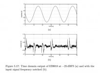
IME Gadget is quite right about ESS recommendations, AVCC regulators, and PCB design. Unfortunately, some of the audible effects are not so easy to measure; not every problem shows up as spurs on an FFT, nor in other common 'figure of merit' tests that an AP machine can do with the push of a button. IIRC non other than Scott Wurcer pointed out there is a problem of over-reliance on 'figure of merit' AP test results. He posted the pic below as an example of a useful but non-standard 'measurement.' I put the word measurement in quotes because there are no studies of correlation between the type of artifact shown and human auditory perception. So we don't know how to interpret the measurement's importance other than by subjective listening tests. Should probably also mention the particular problem shown in the pic is one that does happen to show up on an FFT, but it obviously is not due to static nonlinearity of a voltage transfer function, the type of distortion mechanism that has been correlated with human perception for sine wave test signals (a whole different problem BTW).
Attachments
Last edited:
Indeed Mark. I hadnt even gotten into the IMD hump, which clearly isnt addressed. Not going to be able to do that when you dont know what regulator, layout, exact AVCC voltage and IV opamps people are using. the 9016 doesnt have the feed-forward THD compensation the newer parts do either (which is a bit of a controversial feature anyway, but its not available regardless)
And again making assumptions without knowledge, this time about people. But I'm happy for you that you are so knowledgeable about pcb layout. Btw, the ES9038 datasheet does not specify what you say at al. There is an application note on IV stages for the ES9018.and there lies the problem; you clearly dont understand the significance, or much about PCB layout. Myself, I can actually tell quite a bit about the performance by looking at a PCB; especially for dac parts i'm intimately familiar with. the modular approach in this case and ANY ESS dac, DIRECTLY affects the performance and directly goes against ESS recommendations. the datasheet and application notes specify a direct and low impedance connection to AVCC and IV stage. ....
Now you see what you turned this into? I really wasnt very hard in them in my first comment, but you prompted a much more involved critique 😉 (and i'm still holding back)
The most important for DAC performance is the ground plane:
it should be as solid as possible with as few traces routed through the ground plane as possible. Any traces
that are routed through the ground plane and block the “line of sight” from the DAC output to the opamp
output stage significantly degrades the output THD.
This is then expanded upon. Nothing about power supplies. This is the last I will say about it. I never should have started this.
they ignored that advice too and again. we arent talking about the 9038 (although the same advise follows for that part too)... the first post and every post after is talking about 9016. It's product page is even linked in the first post. YOU started talking about 9038 after I linked the 9016 and mentioned the 9038 in passing ... and keep on referring to it as if its some sort of take down. If you had any experience with the parts and the layouts for them, you wouldnt be making this argument.
AVCC has essentially NO PSRR ... NONE. the measurements I linked, for 9016 (as thats the subject of the thread) show, as he reduced the length of the wires to AVCC, that directly improved performance. does this not tell you something?
AVCC has essentially NO PSRR ... NONE. the measurements I linked, for 9016 (as thats the subject of the thread) show, as he reduced the length of the wires to AVCC, that directly improved performance. does this not tell you something?
Last edited:
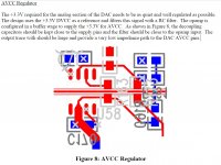
Just to help refresh memories, the document from ESS includes the content copied below about AVCC layout....Nothing about power supplies.
Attachments
Hint, the current for the DAC output comes from AVCC (and, depending, the IV stage opamps). pretty sure they assume they dont need to tell you putting the regs for the most sensitive pins on the board, on another board, on the end of some wires is a bad idea.
aha, yes, there you go, they did mention it explicitly. Thanks Mark.
aha, yes, there you go, they did mention it explicitly. Thanks Mark.
with reference to ground planesJust to help refresh memories, the document from ESS includes the content copied below about AVCC layout.
Is not the AVCC current return path (i.e. the ground plane) a part of the trace impedance calculation?
Had you noticed that both DIYINHK 9016 and 9038Pro boards had only one opamp per cahnnel, so probalby analog part schematic is like this

Yes, but that doesnt change all the recommendations (or the schematic for) for the AVCC regulator, all that remains the same. That is the current topic and that is the image Mark posted. Well, they recommend their own es9311 regulator these days, but layout recommendations should remain consistent. Detail of AVCC circuit is omitted in all 3 examples (its figure 4 in that app note, but since its not on the same board .... plus quite a lot has changed wrt our knowledge of these chips since the es9008).
Expecting a single dual opamp to handle 9038 channel IV, summing and filtering is another very limiting factor. there are not many (ANY?) truly high performance dual opamps that are that low noise and can handle that much current, as well as being fast enough. Maybe opa1622, or a non-standard video, or ADSL driver. Perhaps the good old opa1632, but the whole circuit changes then. but the 1622 wouldnt fit on the board and it has a few wiggles in the response that I want to investigate before recommending it for such a purpose.. In 8 channel mode, the 9038pro puts out around +/-15-16ma. But current requirements of 9016 are much more manageable. I favour a composite opamp in any case.
Mark has a lot of experience with this cheapest circuit for ESS. He mustve modded/bypassed this circuit on 10's of these type of boards; its the circuit favoured by all cheap ebay modders boards. Myself, I havent touched them.
Anyway, what was your purpose for posting this question?
Last edited:
With this schematic ES cannot be configured to current output mode, what gives better THD and noise, also all what is present on AVCC is amplified directly to output.
Yes, you are correct, since you cant achieve the necessary low impedance driving a non-inverting opa input. I wouldn't say thats going to be the limiting factor in this design though. ESS dacs can actually produce a reasonable output even in 'voltage mode', if done well. Not as good as i-out, but respectable all the same, as long as the summing is done properly (which it isnt). I would place that further down the list than the issues discussed so far, but you are correct and the 2 issues together are compounding. I thought you must have something else to add, since just about every ebay ESS dac runs in 'voltage mode' ive even seen them use exactly the same 'IV' schematic on AKM and ESS dacs. the list goes on. look at how far away the decoupling caps are ... not that the ESS eval board is much better in that regard. Theyve made their share of mistakes on their own boards in the past.
I need to make one correction, it does appear that you can install opa1622 on the under side. the pinout for this chip is truly something beautiful and allows such a clean, somewhat symmetrical layout. a missed opportunity and it is capable of the current required; even for 9038 (at least in 8 ch mode). Doesnt solve the other problems, but thats one down at least. Not as supplied, but if you have access to hot air, you can solder it yourself.
Last edited:
Regarding the graph you posted about the hump distortion of the 9018:IME Gadget is quite right about ESS recommendations, AVCC regulators, and PCB design. Unfortunately, some of the audible effects are not so easy to measure; not every problem shows up as spurs on an FFT, nor in other common 'figure of merit' tests that an AP machine can do with the push of a button. IIRC non other than Scott Wurcer pointed out there is a problem of over-reliance on 'figure of merit' AP test results. He posted the pic below as an example of a useful but non-standard 'measurement.' I put the word measurement in quotes because there are no studies of correlation between the type of artifact shown and human auditory perception. So we don't know how to interpret the measurement's importance other than by subjective listening tests. Should probably also mention the particular problem shown in the pic is one that does happen to show up on an FFT, but it obviously is not due to static nonlinearity of a voltage transfer function, the type of distortion mechanism that has been correlated with human perception for sine wave test signals (a whole different problem BTW).
This graph comes up from time to time - I never was sure what this should show and TBH I highly doubt that this is a real measuremen.
Top graph has a resolution of 0.5(Volts?)/div. Bottom graph shows a resolution of 10x that, 0.05/div. The noise there should be clearly visible on the top graph as well. Also the bottom graph shows spikes with a distance of ~2ms - I would not call that HF noise, rather 500Hz which is smack bang in the middle of the audio frequency range. So what's going on there?
for anyone trying to go of this schematic: it is not the IV stage used for the DIYINHK ES9016 DAC. Can't find my notes, but certainly no AVCC connection, no coupling cap and resistors on the output. Just 780 ohm and a parallel cap in the feedback loop (inv), resp to ground (non inv).Had you noticed that both DIYINHK 9016 and 9038Pro boards had only one opamp per cahnnel, so probalby analog part schematic is like this
View attachment 1011111
@Tfive Oh its definitely real. I believe the actual measurement was made by Samuel Groner @scott wurcer has more detail on the setup; I believe it was a time domain measurement and perhaps he may send it privately. He is not only very competent; he has no reason to make this stuff up, as he may have even copped a little professional flack for posting it, so I wouldnt ask him to comment or post publicly. Its not the same as the IMD hump we experience with the newer models. He does discuss it in more detail somewhere here and also on ASR, but perhaps he can chime in here, or perhaps PM myself or you. Not so relevant now anyway, more of an academic interest.
- Home
- Source & Line
- Digital Line Level
- 8-channel DAC + board for low-power application