Congrats, Ling. It's a big process to get through. I look forward to the results! Thanks for all your work on this.
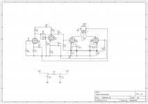
Drew up the schematic of the 6AS7 output stage, all just for you
Ignore the notes on the 1306:4 ohm toroidal, should read 1306:8 also
View attachment 659353
Same front end that I used on this amplifier, just with a red LED instead of a cathode resistor for the input tube, and open loop (no feedback). Were I to do it again today I would also load the input tube with a CCS for more output swing. The important thing to keep in mind here, is that the input tube and phase inverter need around 300 volts to give acceptable performance, so what I did was rectify both secondaries of a dual primary/dual secondary toroidal isolation transformer, and stack them on top of eachother, giving both 160 and 320 volt supply rails. Worked great, cheap, simple. I liked it so much I built up a five channel version years ago, and might build another with toroids this year.

Hi Ling. Can you explain the 2 level PS for the 6AS7 a little more? You first rectified each section of the transformer, THEN stacked them? Or stacked them right off the secondaries, then rectified the two outputs for the two B+ values? I've never tried either and am getting stuck on the theory for how it works. Thanks! BTW, I may run some drivers at the same B+ as the 6AS7 but drive an interstage for the proper swing. So I'm looking at different driver tubes than the 6SL7. But I'd still like to understand what you did.
Carl
Basically like this-
Two 120 volt secondaries, each rectified to 160 or so volts, and stacked to give 0, 160, and 320 (or +160, 0, and -160, depending on how you look at it) pretty much. You can also do a single 120 volt transformer with a 6 volt heater winding, and run a small 120:6 transformer backwards off of a heater winding and stack that the same way.
Two 120 volt secondaries, each rectified to 160 or so volts, and stacked to give 0, 160, and 320 (or +160, 0, and -160, depending on how you look at it) pretty much. You can also do a single 120 volt transformer with a 6 volt heater winding, and run a small 120:6 transformer backwards off of a heater winding and stack that the same way.
... I have already commenced buying parts. 🙂 I'm looking forward to making one of these. In the spirit of the amp, I'll be using 100V PA tansformers for outputs and I'll be bodgying up something for the power transformer.
I'll be using it for a headphone amp in due course - nothing quite like a grossly overengineered solution where an opamp and a buffer would do... 😀
I'll be using it for a headphone amp in due course - nothing quite like a grossly overengineered solution where an opamp and a buffer would do... 😀
Basically like this-
Two 120 volt secondaries, each rectified to 160 or so volts, and stacked to give 0, 160, and 320 (or +160, 0, and -160, depending on how you look at it) pretty much. You can also do a single 120 volt transformer with a 6 volt heater winding, and run a small 120:6 transformer backwards off of a heater winding and stack that the same way.
OK, thanks!
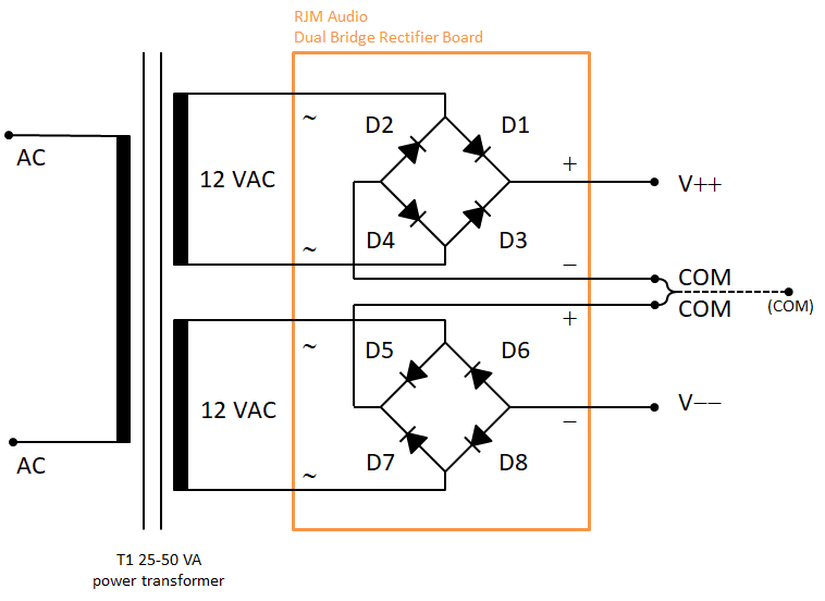
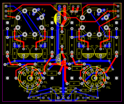
Just realised that I never shared the absolute-final-draft of the board, here's the renders-
(couple minor silkscreen issues, but no worries)
Also- Just got my shipping notification, they are due to be delivered this wednesday!!!!!
HYPE!!!!!
(couple minor silkscreen issues, but no worries)
Also- Just got my shipping notification, they are due to be delivered this wednesday!!!!!
HYPE!!!!!
Attachments

Not yet. Should have the first run of ten in hand tommorrow, then after sending a few out and building them up to verify function I'll start up a group buy thread to take real orders after implementing any suggestions or fixes. I'm pretty excited 🙂
I have everything needed to put a pair of these together. A way to make about 325V B+, some 6SN7s and a couple of 6SL7s. The Antek transformers aren't pricey, so this would make a KILLER headphone amp. I even have a few 6AS7Gs and 6080s, and maaaaybe a pair of 6336 (!!!) -- for if I just HAVE to make a speaker amp out of it.
(and thanks for your suggestions on the 150V DC pwr supply thread...)
(and thanks for your suggestions on the 150V DC pwr supply thread...)
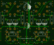
Boards came in!
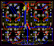
They look fantastic! Just a few minor goofs on the silk on my part, but they look like they will work great! I'll get one stuffed and tested before I send any out, but just as I go I don't see any obvious errors. I'll give a write-up tomorrow morning hopefully.
They look fantastic! Just a few minor goofs on the silk on my part, but they look like they will work great! I'll get one stuffed and tested before I send any out, but just as I go I don't see any obvious errors. I'll give a write-up tomorrow morning hopefully.
Attachments

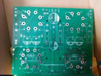

For anybody considering using JLCPCB, I ordered these Friday night, and received them Tuesday afternoon 😱 That is a crazy fast and affordable turnaround.
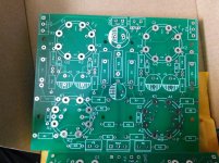
Also, I started on the board last night, but only got as far as the screw terminals and a few caps/resistors before I had to put it all away for daddy stuff with the family. Hopefully I can get more done tonight. So far it solders beautifully. I'll be making notes as to what I think needs to be modified for the next run/revision, but as is they seem to be a very usable board. This first board is getting the "whatever I have on hand" parts treatment, with a few tricks to make it easy to swap parts around 🙂
Also, I started on the board last night, but only got as far as the screw terminals and a few caps/resistors before I had to put it all away for daddy stuff with the family. Hopefully I can get more done tonight. So far it solders beautifully. I'll be making notes as to what I think needs to be modified for the next run/revision, but as is they seem to be a very usable board. This first board is getting the "whatever I have on hand" parts treatment, with a few tricks to make it easy to swap parts around 🙂
excellent sir.....now if you would please ....would you be so kind and post the BOM
Thank you
Lawrence
Thank you
Lawrence
Working on that soon. It's a pretty flexible design so it'll have notes as to alternatives for many of the parts values. I really wish I had a way to draw up a nice annotated schematic with the BOM and notes, but haven't found anything I like for that yet.
It should be a relatively easy project to draw up variations for different tubes (I've been thinking about a few tube possibilities including 12B4 which would require a bit of a re-working). Maybe those who do that would consider posting what they came up with and a BOM for the signal circuit. The signal BOM should be relatively short. Maybe a description of the PS you use would also be helpful.
So, here's the pretty much current schematic. Parts values listed assume an approximate 285-290v supply after power supply filtering- I guess this is the start of a user guide of sorts!
R1- 220K. anode load resistors, a 1/4w part will work, I recommend a 1/2w part. Could go lower to 180~200K if the cathode resistor is adusted to give 50~60% of the supply voltage at the anode.a corresponding change in the feedback resistor may be required, but only if you are concerned about exact ratios.
R2- 1K. Grid stopper. Anything from 220R~1500R will work, non critical. Might even be left out if using short interconnect.
R3- 100K. Grid leak. Also non critical. Just don't go too high. If using a control pot ahead of it, size it to be anywhere from six to ten times the value of the pot. I don't recommend going higher than maybe 250K to ground here, however due to grid capacitance. A 10K pot with a 100K resistor will work well.
R4- 2700R. Cathode resistor. Unbypassed. May need to adjust larger or smaller to get to a good operation point at the anode. 220K anode with 2700R cathode, and 27K~39K feedback resistor seems to work very well for me using the Russian 6N9S at around 285-300 volt supply.
R5/R6- 1M. Step network. Sets bias for concertina splitter. R5 is assumed to be 1M if the preceding plate voltage is 50% of the supply voltage. Going forward it may be better to use 1.5M for R5, and adjust the previous stage for around 60% or so of the supply voltage to provide more symmetrical swing. The goal is to see 25% of the supply voltage at the cathode of the concertina either way, but it's not super critical at the signal levels we are seeing. Anything from 20~30% will also work.
C1- 100nF. coupling capacitor. This shorts the signal across R5 to allow a lower DC bias voltage, without reducing the AC signal. A quality polypropylene or polystyrene cap will do great here, and a 250V rating is plenty. I like axial lead types, but the board will also take 15mm lead spacing box types as well. You could go as low as 10nF here if you like, as we aren't making enough power to push much bass types of signal anyway.
R7/R8- 100K. Concertina load resistors. Try to get these as closely matched as possible, this will ensure the best balance of drive signal. You can also go to a 68K~75K if that's what you have, but don't go much lower or performance will suffer. 1/4w is fine, I would even say that 1/8w would be fine in a pinch, but that's up to you.
C2/C3- 100nF. Coupling capacitors. Same advice as for C1. C1, C2, and C3 can all be identical for ease of sourcing parts.
R9/R14- 1M. Output stage grid leaks. These can be as low as 220K really, but I like to keep them large to ease the load on the phase splitter. I usually use a 470K or a 1M here. Non critical as long as they aren't too small.
R10/R11/R12/R13- 1K. Cathode/Garter bias resistors. 1/8w will work here, but I would rather see a 1/4w or 1/2w part here. These should be very tightly matched as well, and done in pairs if you are unable to do them all per channel, IE, R10/11, and R12/13 should be closely matched so that side-by-side the track as best as possible. You can also go lower resistance here if you like, at the cost of higher dissipation in the output stage, 680-820R perhaps. Watch the max dissipation here though, and be sure to use "GTA/GTB" types if running them hot.
C4/C5- 470uF. Bypass caps. Use a 25-35v part here, low ESR preferred. You can go lower in value to about 150uF without a noticeable lack of bass, but I wouldn't go lower than 220-330uF personally. Going up to 1000uF wouldn't hurt, but wouldn't be a huge benefit either unless it's parts on hand already.
R15- 27K. Feedback resistor. Could go higher or lower to taste, or as needed to make up for lower output signal sources. Going higher than 47K doesn't seem to work as well as something around 22K~39K, with my personal favorite being 27K from what I've tried.
R16- 1K. Power supply filter resistor. Optional, depending on your choice of PSU. May or may not be needed in some applications. Might be replaced with a wire link if using a regulated supply.
C6/C7- power capacitors. 47uF each on the schematic, but realistically you can run 10uF~22uF for C7, as the front end draws such low and constant current. May also be omitted in some applications.
T1- output transformer. This one's a bit tricky. I use a 10VA power Toroid, with parallel connected 5 volt secondaries, and the dual 120 volt primaries connected in series, with the connection being used as the center tap... Used this way it presents an approximate 17K plate-to-plate load. If using a conventional transformer, look for a 16K-20K load. This can easily be accomplished by using a standard EL84 or 6V6 output transformer from 8K-10K, and running twice the nominal load impedance on the secondary, IE, an 8 ohm load on a 4 ohm secondary. If not using feedback a higher load impedance is better than lower.
On the PCB side of things-
I got the board mostly stuffed, and found I was out of 1K resistors, so I had to stop for the night. I'll try and grab some locally tommorow if possible. I'm happy to say that the board is pretty easy to use, as intended so far 🙂
I also started on a noval input version of the board, stay tuned for more details...
Attachments
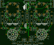
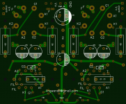
Sneak peek at the noval input version of the board, should allow greater flexibility for using alternative output tubes, like the 6336A, 6AS7G/6080, etc. a 6N2P front end should provide plenty of swing, even with an unbypassed cathode for the 6AS7G. Also gives the option of using 12AX7, 12AT7, 6DJ8 types, etc. Should be a nice flexible board.
Since the sockets are smaller up front, I was able to rearrange some of the resistors for a more symmetrical and pleasing layout, which gives me a warm and fuzzy 🙂
I'm currently thinking, that in order to streamline things a bit I may finish the noval version and order boards too, that way those testing can try out one of each. This will save a bit of hassle on my part for shipping, and wont add too much of a wait seeing as the turnaround from having the boards made is so quick. Any objections?
Also, any features that you guys would like to see implemented? The noval version has a little bit of board real estate available up in the front/bottom corners, so I was toying with the idea of adding the circuitry for a 10M45S or maybe DN2540 cascode CCS in the corners for experimenters, and maybe even adding the pads for LED bias for those who may wish to use it, as it would be pretty easy to jumper across them at build time if it isn't desired.
Attachments
- Home
- Amplifiers
- Tubes / Valves
- 6SN7 push pull flea amplifier project