Is it ok to keep the development of the boards here, and then start a new group buy thread once I order some and start doing that side of things?
 Of course, whenever you are ready.
Sweet. I'll start a new thread over there once the boards are ordered.
I didn't get a chance to mess with anything DIY last night, so we'll see how things go tonight. I have a couple minor changes, and some tracks getting switched a bit, but I think it's mostly done otherwise.
I didn't get a chance to mess with anything DIY last night, so we'll see how things go tonight. I have a couple minor changes, and some tracks getting switched a bit, but I think it's mostly done otherwise.
Can you do a quick mspaint or similar circle/arrow pointing to what you mean? I'm not certain I follow...

My apologies for the looseness of my description. I shall therefore be more explicit, at the risk of seeming brusque or didactic. Please understand that such is not my intent, merely clarity of communication.
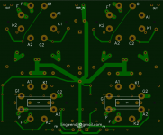
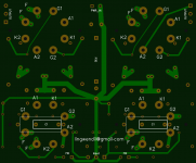
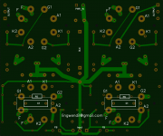
One end of C2 is connected to the anode of V2; that node is close to B+ in voltage. My guess was 3/4 B+ for symmetrical upper and lower swing from V2. That trace is on the top layer. There is a fat ground trace on the bottom layer underneath, routed near the pad where C2 connects to the PCB at that end.
Because the pads for C2 are instantiated on the top and bottom layers, there is a very small gap on the bottom layer between copper carrying a couple hundred volts (C2 pad) and copper tied to ground. I have drawn a circle in lavender centered on the area to which I refer. I don't have a measurement of that gap, but it looks small and could easily be wider.
Just thinking about AC signals on various traces, I'm wondering about the proximity of traces to pads on the output connector for V3 as well. Seems like those anodes will be generating some fairly high-voltage swings, out of phase, and so the instantaneous voltage difference between those two may also be a few hundred volts. I would prefer a larger gap between the left trace and the square pad, and I can't see the harm. However, not being the designer, I can't claim to have all of the design variables under consideration.
Those are the kinds of things that I would nudge and tune on a final inspection pass; not any need to make those clearances so tight in either place, and easy enough to open them up - so I would do so, were it _my_ final polishing pass. There are probably several other places that you or I could find where some gentle nudges would ease some voltage gradients, or keep noisy traces away from quiet ones, or at least orthogonal to them.
See, this is exactly the sort of constructive commentary I was looking for! Not brusque at all. Like I said, I'm new at this. I definitely see what you mean now with the ground trace being so close to the pad, so that's an easy enough fix. Same with the output terminals, I'll get those traces spaced away from the pins a bit better too. Way easier to do now than later 😉
Great work!
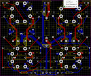
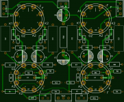
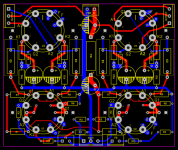
If the black dots at the sides of octal sockets are the mounting holes for the board, It seems that the bottom ones are near to other components. Is there enough space to fit hexagonal standoffs without having them interfere with pads or resistors?
Some octal socket pads are almost touching the side of the board. This should be avoided because there is a risk of shorting the pads to ground if someone will try to fit the board in a narrow metal enclosoure.
I also have a suggestion: the routing of the transformer cables is cleaner when the connections are grouped togheter. Maybe you could fit two 5-pole pluggable terminal blocks, one for each channel, to group the 5 transformer wires (3 primary + 2 secondary). This way the output transformer wiring will be a easier task for beginners, and amplifier servicing will be faster.
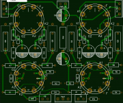
It may be helpful to view only one layer at a time, making it easier to see where things are close.
Great work!
If the black dots at the sides of octal sockets are the mounting holes for the board, It seems that the bottom ones are near to other components. Is there enough space to fit hexagonal standoffs without having them interfere with pads or resistors?
Good catch. R2 should have plenty of room, R6 looks a bit too tight. I'll scoot both a bit to give more clearance. Hex standoffs with 4-40 or M3 are what I usually use, so I'll want them to fit!
Some octal socket pads are almost touching the side of the board. This should be avoided because there is a risk of shorting the pads to ground if someone will try to fit the board in a narrow metal enclosoure.
Hmm. I think it may not be a terribly big deal, since most sockets overhang by just a hair when you look at them from above, due to the casting of the porcelain. Either way I'll see if I can scoot it half a grid or so down just to be safe.
I also have a suggestion: the routing of the transformer cables is cleaner when the connections are grouped togheter. Maybe you could fit two 5-pole pluggable terminal blocks, one for each channel, to group the 5 transformer wires (3 primary + 2 secondary). This way the output transformer wiring will be a easier task for beginners, and amplifier servicing will be faster.
Hmmmm. My original intent was to have the transformer center taps feed right off of the power supply (preferably at the reservoir cap) and left the connection off board to allow the use of separate driver and output supply voltages- for example, when using 6SL7 front end off of 300 volts, and a 6AS7G output stage off of 165 volts supply. I suppose it wouldn't be too tricky to route a main supply voltage trace next to each block, and change the blocks to 3 pole screw terminals, that would allow easy enough wiring per channel/transformer, and I could remove one of the power supply input terminal blocks at the top of the board. Does that sound like it would be a good idea? That way we have power/ground in on one block, and anode/power/anode terminals for each output tube. Keeps it easy with each tube's transformer having its own separate easy-to-follow connections, and simplifies the power wiring for most basic builds. I still like the idea of separate terminal blocks per channel to keep it easy to follow.
I'm not terribly familiar with pluggable terminal blocks, do you have an example of the kind you mean? If they have them in the same lead spacing it might not be too difficult to work them in.
It may be helpful to view only one layer at a time, making it easier to see where things are close.
I've done that a bit, but admittedly not as much as I should. After some changes I'll start going through and doing so to verify.
Also, I'm thinking of removing the VCC_OUT connector at the bottom, and going to a single center bottom 3P terminal block for the input, it'll take a bit of moving things around, but it'll let me scoot most of the circuitry down a bit, and I'll rearrange the FB connections slightly. Any objections? I think it'll be a bit easier to deal with and less work at wiring time.
Man, once this is all finalised I'm going to start on the PSU companion board, that will be ten times simpler 😉
Last edited:
Your idea about the 3 pole terminals is good. When I use PCBs, I try to mount them in a way that will ease the removal from the chassis for inspection and modification, without the need to desolder or unscrew wires. Wurth terminal blocks and PCB spade connectors are a cheap and easy way to achieve this goal. For signal and low voltage connections, I use Molex C-Grid III connectors. All three kind of connectors are available as straight or side mounting.
Attachments


^ Those are definitely interesting for sure. I'll do a bit more research on them, and maybe order some to try out. If i like them i might incorporate them eventually.
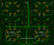
I'm trying to figure out how to easily fit 3P terminals for the outputs, but here we are so far. I might just turn them sideways, and face out the sides of the board... Moved a few things around, consolidated down to a 3P terminal for the input, and did a little bit of minor rework. Got the top sockets down a bit too. I don't think I'll mess with the cathode/feedback resistor arrangement, since it doesn't seem that there are enough options for octal dual triodes to make it all that worthwhile for experimenting. I really wish there was a common octal with a mu around 30~35, but maybe I'll make a later revision for nine pin inputs that will have a few more bells and whistles 🙂
I'm trying to figure out how to easily fit 3P terminals for the outputs, but here we are so far. I might just turn them sideways, and face out the sides of the board... Moved a few things around, consolidated down to a 3P terminal for the input, and did a little bit of minor rework. Got the top sockets down a bit too. I don't think I'll mess with the cathode/feedback resistor arrangement, since it doesn't seem that there are enough options for octal dual triodes to make it all that worthwhile for experimenting. I really wish there was a common octal with a mu around 30~35, but maybe I'll make a later revision for nine pin inputs that will have a few more bells and whistles 🙂
Attachments

Last edited:
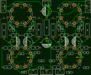
Oops, forgot to attach the multi-layer (ignore the ratlines). Also forgot to add, I added a larger footprint to accommodate more capacitor types under the input tubes. I've only really kept in mind axial capacitors for the coupling caps, are there any other types that people would like included? I see MKP film types on many board designs and BOMs, but not too many on p2p types of builds, so I wasn't sure if there was enough demand for them.
Attachments
Last edited:
Yep. Should work just fine, as they are electrically equivalent in this use. Only issues for this board will be they will require the cathode resistors to be mounted offboard due to size, as the boards are meant to be optimised for the 6SN7 and similar size/power tubes. if using the 6AS7G/6080 typesthe cathode resistors will be dissipating several watts each, so use of at least a 5, but better a 10 watt resistor would be reccomended. Also, due to their rather large size the tubes themselves wil be pretty cose together, and proper care to ventilation of the chassis will need to be kept in mind.
Not a big deal, just something to keep in mind.
Not a big deal, just something to keep in mind.
On my build I used Vishay MKT373 100nF 630 Vcc capacitors as C1, C2 and C3: 6 identical capacitors, to keep things simple. Terminal spacing is 15 mm.
On my build I used Vishay MKT373 100nF 630 Vcc capacitors as C1, C2 and C3: 6 identical capacitors, to keep things simple. Terminal spacing is 15 mm.
I'll see if those are in the library and if I can work them in.
Alright, more fiddling. Got the 3P output connectors fitted in. Since the board is so small I switched them sideways, and you can mount the terminals top or bottom, facing in or out. Should work out pretty well for any conceivable need!
Attachments
C4 and C5: if you rotate them each 90degrees such that the positive terminal is to the North and negative to the South, you can route the ground trace from the star point further to the south. That will leave more clearance and shorten the traces from cap to tube. You might even move R13 and R14 south and move C4 and C5 to their north, simplify the topology even more. Even better, perhaps, might be rotating R13 and R14 each 90 degrees and put them beside C4 and C5, with all four parts' ground connections on the south side. Either way, I think C4 and C5 are a bit close to the tubes.
I might rotate C7 90deg CW for the same reasons.
I might rotate C7 90deg CW for the same reasons.
The caps are meant to be mounted on the bottom of the board, but I see what you mean as far as simplifying the ground trace by scooting/swapping R13/14 and C4/5. You mean the two caps next to eachother, with the two resistors out on either side?
I'll save a copy and try that out and see how it looks. For C7 I assume you mean rotate it clockwise 90°? Thanks!
I'll save a copy and try that out and see how it looks. For C7 I assume you mean rotate it clockwise 90°? Thanks!
Last edited:
Alright, if this is what you meant, I like it. I think it looks pretty good, and at such short runs I'm willing to go to a nice thick trace for ground right to the reservoir cap instead of the star ground type I had going before. Unless there are any objections I think I'll go with this style from now on.
EDIT- Crap! I keep forgetting it renames parts when I copy-paste over groups lol. It's fixed now. Just not in the pics.
EDIT- Crap! I keep forgetting it renames parts when I copy-paste over groups lol. It's fixed now. Just not in the pics.
Attachments
Last edited:
- Home
- Amplifiers
- Tubes / Valves
- 6SN7 push pull flea amplifier project