I actually thought, and I would have liked, that we would use the simulator for this.
MC12 tells us very precisely that the MF-A1 switches from true A mode to AB mode from 14.025V pk under static 8 ohms (steady state).
That is just under 12.3 real watts.
thx wahab!
MC12 tells us very precisely that the MF-A1 switches from true A mode to AB mode from 14.025V pk under static 8 ohms (steady state).
That is just under 12.3 real watts.
thx wahab!
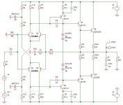
Now back to the magical dimensioning of Z1, Z2, Z3 and especially Z5 - that would make me very happy.
After all, this is where esotericists see the magic of A1 hidden.
After all, this is where esotericists see the magic of A1 hidden.
That is yet another completely different area that needs to be improved.not counting
less than 10 damping factor, not that 18-19 on 8R was already a great number.
A small, marginal correction, I ignored the internal resistance when taking my values ..!I actually thought, and I would have liked, that we would use the simulator for this.
MC12 tells us very precisely that the MF-A1 switches from true A mode to AB mode from 14.025V pk under static 8 ohms (steady state).
That is just under 12.3 real watts.
thx wahab!
10.97 W RMS
This is 13.25 V pk as the limit of A operation. Iq is 808mAdc in idle mode, just as an indication, nothing more.
Class A mean nothing if this amp produce roughly 40dB higher THD + IMD at 10W RMS than a same transistors count
regular symmetrical differential amp biased at 55mA, that s just some incantation deprived of any technical ground.
Indeed thanks to the class A non sense the marketers are promoting vastly inferiors amps, they know too well
that A sound first rate even if it s rubbish design and that AB and B sound like second rate and are perceived
psychologicaly the same way as B series film or financial AB and B credit ratings.
A1 vs. Class B blameless design:Class A mean nothing if this amp produce roughly 40dB higher THD + IMD at 10W RMS than a same transistors count
regular symmetrical differential amp biased at 55mA,
0.2% worstcase at 10W
-40dB thd means now 0.002%

Eventualy, if you are content with Purifi s 3.5V/us, those class D are a first, for the first time an average tweeterThen D.
has better slew rate than a recent transistored and ICed amp.
A1 vs. Class B blameless design:
0.2% worstcase at 10W
-40dB thd means now 0.002%
As i wrote it not even a blameless but a symmetrical differentals with same transistors count and quite less components overall
than the MFA1, the one below, let alone if it was a blameless or a refined symmetrical :
Attachments
I explored the idea of regulating the output transistor's idle current in a separate feedback loop a long time ago. Back then I used a single sense resistor on the collector of the PNP EF output stage (I used a variation on a current mirror using a super-match NPN pair to do the job). The problem: the amplifier was a class AB design so the average current varied substantially, depending on the source material. That "little" problem only revealed itself when I was test-driving the design. At the time I wasn't interested in class-A amps so dropped the idea.
I concluded that sort of "auto-bias" scheme could only work in a pure class-A amplifier where the average current flow through each output device was invariant w/respect to the source material. I considered an approach that sampled the idle current around the zero-crossing point (which would work OK for class AB) but just didn't want to go down that road. This was in the '70's or maybe early 80's.
The fact that the class A's average idle current won't change, despite what kind of signals are applied to the load, establishes the idle current needed: it must be sufficient to meet the power-out specification for that particular design. P = I^2 R. Beyond that, the average idle current will change if the amp enters a class-B operating mode (and if it's capable of sourcing excess current). For my design, since it only sensed one of the output transistors, the idle current setpoint would drift down because the average, sensed, current would trend upward. The A1, while it incorporates current sensing for both output transistors, would behave in a similar fashion (because each device's idle curent is sensed). If the current-sense signal is NOT lowpass-filtered, the current-sense feedback path will play a role in the amplifier's realtime behavior. Not necessarily a good thing.
The earthquake began here. Iq 700mA.As i wrote it not even a blameless but a symmetrical differentals with same transistors count and quite less components overall
than the MFA1, (...)
The difference between the THD comparisons is no more than 20dB over the thumb. In other words, a decimal point shift of a single digit. User wanted to outline that with the same number of (counted) transistors and the classic IP-VA-OPS (OPS formed as EF) you can basically write a better THD value in the specifications. There is a very simple technical connection for this, which you can read about in the original thread. However, it is irrelevant in this thread.
Maybe the MF company probably wanted to counter the Japanese mass invasion of really quite good audio amplifiers in the early 1980s. We all probably remember the usual discussion about TIM, PIM, TID, low feedback, etc.pp.Class A mean nothing if (...)
I can't see anything wrong with that.
One should not judge the MF-A1 (which we may regard as the originator of the “3/4 + 3/4 Amplifer”) prematurely by its technical data alone, one should test it extensively by listening to different loudspeakers. At my home, the 2023 model is currently playing non-stop with a two-way loudspeaker. This DIY LS with a (very low-cut) Visaton B200-6 is not dissimilar to the Borg. The sound is phenomenal.
If we are honest, the so-called transconductance output side is responsible for the fact that the technical data of the MF-A1 is only ever a worst-case scenario.
This is because the no-load gain (SE-OLG as well pp case) is ultimately dependent on the amount of working resistance and we do not know this! Of course, an infinite open-circuit amplification of the system would later lead to a load-independent amplifier. The 3/4 + 3/4 approach would like to use this basic positive mechanism of negative feedback to its advantage. OLG is high!
In the 1980s, MF did not specify the THD of the A1 and casually stated it as 0.5% worst case. And this is exactly the right thing to do if you don't want to print extensive profiles that would have to be explained to the potential buyer in a technically correct way.
HBt.
Addendum
And I hope we can get back to the design, i.e. the suggestions of @jxdking and my overkill posting #1. Up to 2+1/4 real watts, i.e. already more than high room volume, every A1 is a player without fault.
Many thanks also to Mark'51 for his contributions so far, great ...
Last edited:
The earthquake began here. Iq 700mA.
The difference between the THD comparisons is no more than 20dB over the thumb. In other words, a decimal point shift of a single digit. User wanted to outline that with the same number of (counted) transistors and the classic IP-VA-OPS (OPS formed as EF) you can basically write a better THD value in the specifications. There is a very simple technical connection for this, which you can read about in the original thread. However, it is irrelevant in this thread.
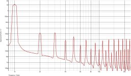
In the FFT i posted the main signal and the higher harmonics, H2 and H3, are 100dB apart, that s 40dB lower than the MFA1
that manage hardly -60db THD at 10W, beside that s at 55mA Iq.
Maybe the MF company probably wanted to counter the Japanese mass invasion of really quite good audio amplifiers in the early 1980s. We all probably remember the usual discussion about TIM, PIM, TID, low feedback, etc.pp.
I can't see anything wrong with that.
The "mass invasion" began earlier, in the late 70s, FI Hitachi s lateral FETs amps are from 1978 like JVC s non switching Super A,
by 1980 the 2SA1302/2SC3281 were ubiquitous and it was already over for EU and US brands.
To counter the japanese technical excellence far more than this outdated design using antic power transistors would had been necessary, it was some kind of third rate imitation of Accuphase amps but without the seriouness in design and was just directed
at the gulllible that had no technical knowledge at all.
Indeed the article you linked say that the designer specialty was tube amps and that say it all, his amp beg an output
transformer to match the OS high Z output with speakers low impedance, actualy this is reminiscent of amps where
the two windings of a transformer are driven by two same polarity transistors in common emitter mode, that is, at
high impedance, the same way as tube s outputs.
That is what Mr. M. Kühne assumes - correctly.Indeed the article you linked say that the designer specialty was tube amps and that say it all, his amp beg an output
transformer to match the OS high Z output with speakers low impedance, actualy this is reminiscent of amps where
the two windings of a transformer are driven by two same polarity transistors in common emitter mode, that is, at
high impedance, the same way as tube s outputs.
Unfortunately, we are no longer able to ask Mr. Tim de Paravicini about this. As you know, all this is insignificant for our self-build hobby.
Apart from this, the output resistance of the two-stage system is correspondingly low as soon as it is feedback'ed - counter coupled globally ---> nfb.
right,In the FFT i posted the main signal and the higher harmonics, H2 and H3, are 100dB apart, that s 40dB lower than the MFA1
your {3 * f one} is -60dB apart ..!
I agree with you 100%, that's exactly how I rate this review as well.o counter the japanese technical excellence far more than this outdated design using antic power transistors would had been necessary, it was some kind of third rate imitation of Accuphase amps but without the seriouness in design and was just directed
at the gulllible that had no technical knowledge at all.
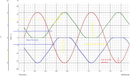
The deformations on the signal edges (and also the points in time) before the addition at the output node can be seen very clearly.At 0.8A bias the OS largely switch off for 2A pk output current, unless one consider 70uA residual current
as being still switched on, we can see that switch off occur at 1.6A, wich is exactly 2 x the bias Iq and 10W RMS.
I took the liberty of doodling around a little in the graphic.
The famous first watt is flawless. Up to five real class A watts, it also remains largely flawless.
Attachments
Last edited:
My final side note on the original:
I'm starting to get excited about MC12 after all, because this tool is very powerful in a simple way. It lets us find the exact limit of A operation of an MF-A1 and this is at an initial DC quiescent current of 808mA at 8.23W rms at a static load of constant 8 ohms. According to my simulation with MC12.
Who would have thought it?
Obviously, the disguised autobias is not really a brilliant idea after all. Or perhaps the dimensions of the bridge elements Z1, Z2, Z3, Z4 and Z5 are not optimal.
Whether 3/4 + 3/4 will perform better 😉 ?!
The deformations on the signal edges (and also the points in time) before the addition at the output node can be seen very clearly.
I took the liberty of doodling around a little in the graphic.
The famous first watt is flawless. Up to five real class A watts, it also remains largely flawless.
There s actualy no image deformation, that s due to the jpeg image converter as the original pic format
is not supported by DIY Audio images storage.
Beside, the famous 1st watt is a wrong conception as it imply that dynamic range is very limited, as well as homogenous
speakers efficency, a better basis is the DIN 45500 2 x 6W RMS, and that was still with reduced dynamic ranges of the time.
- Home
- Amplifiers
- Solid State
- 3/4 + 3/4 the strange A1